Line Scan Lens Application for Silicon Wafer Appearance Inspection
With the vigorous development of the solar photovoltaic industry, the quality and stability of photovoltaic silicon wafers, as the core material of solar cells, have attracted more and more attention. It is particularly important to conduct appearance inspection of photovoltaic silicon wafers.
There are many types of appearance defects in photovoltaic silicon wafers, common ones include cracks, scratches, bubbles, dust, etc. These defects not only affect the aesthetics of the silicon wafer, but more seriously, may cause the battery power to decrease or even fail. Therefore, timely detection and elimination of these defects to ensure the quality and stability of silicon wafers is of great significance to improving the power generation efficiency and extending the service life of photovoltaic cells.
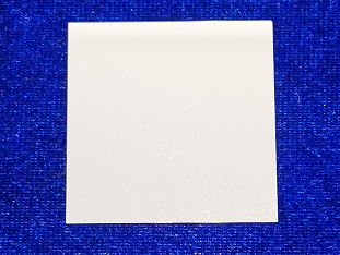
The visual inspection solution of industrial lenses matched with industrial cameras is widely used in silicon wafer appearance inspection and can quickly and accurately detect surface defects. However, there are many types of industrial lenses on the market. Which type of lens should be chosen to complete the inspection efficiently and accurately?
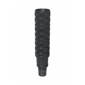
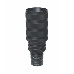
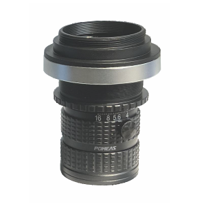
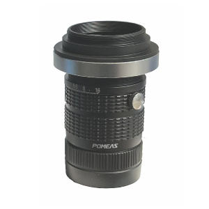
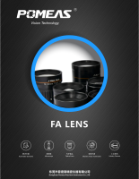
POMEAS' new line scan industrial lens has the advantages of high speed and high resolution. When used in vision solutions, it can obtain high-quality silicon wafer surface images, clearly and quickly identify appearance defects, and improve detection efficiency and accuracy.
Line scan industrial lenses have the following advantages:
1. High-speed scanning: The line scan lens can scan the entire silicon wafer in a short time, greatly improving detection efficiency.
2. High resolution: The resolution of line scan lenses usually reaches thousands of pixels, which can capture tiny defects and accurately locate and identify them.
3. High degree of automation: Line scan lenses combined with image processing software can achieve automated detection, avoiding the subjectivity and errors of manual vision.
4. Strong adaptability: Line scan lenses can adapt to different inspection needs and can be adjusted and optimized according to different defect types.
Product recommendation
TECHNICAL SOLUTION
MORE+You may also be interested in the following information
FREE CONSULTING SERVICE
Let’s help you to find the right solution for your project!




 ASK POMEAS
  PRICE INQUIRY
  REQUEST DEMO/TEST
  FREE TRIAL UNIT
  ACCURATE SELECTION
  ADDRESS
 Tel:+ 86-0769-2266 0867
 Fax:+ 86-0769-2266 0867
 E-mail:marketing@pomeas.com
