


How to select a telecentric lens to meet specific measurement requirements?
POMEAS not only offers a full range of telecentric lens products but is also committed to providing customers with professional selection guidance and technical support....
How do telecentric lenses enhance the efficiency of measurement solutions?
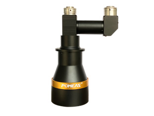
The POMEAS telecentric lens employs a specialized optical design and coating process to deliver exceptional resolution while maintaining a large depth of field....
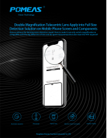
What are some typical applications of telecentric lenses?
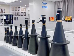
POMEAS telecentric lenses have been successfully applied across multiple industries including 3C electronics, semiconductors, new energy batteries, and precision injection molding, providing custom......
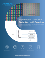
What are the advantages of telecentric lenses in measurement solutions?
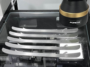
Telecentric lenses offer high precision advantages in measurement solutions, eliminating measurement errors caused by parallax in traditional lenses. They also ensure more stable imaging performanc......
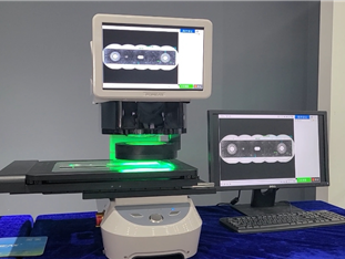
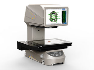
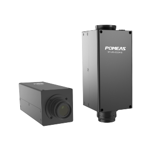
What is a high-precision image dimension measuring instrument?
POMEAS has evolved into a specialized manufacturer and solution provider of high-precision image dimension measurement instruments....
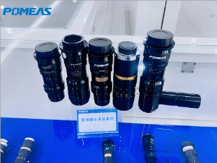
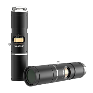
What is an industrial ZOOM LENS?
Industrial ZOOM LENSes are specialized optical imaging devices designed for industrial applications. They achieve continuous magnification changes by adjusting the focal length of the optical system....
Four Key Questions About Image Dimension Measuring Instruments
What are the four major questions about image dimension measurement instruments? How exactly do they achieve non-contact measurements with sub-micron precision in an instant? Read on to find out....
Five Key Questions About Spectral Confocal Displacement Sensors
Five Essential Questions for Beginners About Spectral Confocal Displacement Sensors: How Do They Achieve Nanometer-Level Non-Contact Measurement?...
Product recommendation
TECHNICAL SOLUTION
MORE+You may also be interested in the following information

FREE CONSULTING SERVICE
Let’s help you to find the right solution for your project!

 ASK POMEAS
  PRICE INQUIRY
  REQUEST DEMO/TEST
  FREE TRIAL UNIT
  ACCURATE SELECTION
 - APPICATION CASE
- RESOURCE CENTER
- DOWNLOAD CENTER
SOLUTIONS SUPPORT
- ZOOM LENS SELECTION TOOL
- TELECENTRIC LENS SELECTION TOOL
- FA LENS SELECTION TOOL
- ZOOM RATIO TABLE
- CERTIFIED MODEL
SELECTION TOOL
- WHY POMEAS
- FAQ
- PRIVACY POLICY
- TERMS OF USE
- DELIVERY & RETURN POLICY
CUSTOMER CARE
 ADDRESS
Add.:No.68, Yongwei Road, Baizhoubian, Dongcheng District, Dongguan, China,523000
CONTACT
 Tel:+ 86-0769-2266 0867
 Fax:+ 86-0769-2266 0867
 E-mail:marketing@pomeas.com

Wechat QR code
Software Copyright :2021SR0176001 抄袭必究, 技术支持:誉新源科技