
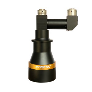
Application of Telephoto Lenses in Online Dimension Inspection of Precision Components
Telecentric lenses have become the standard component for online dimensional inspection of precision parts due to their core advantages of low distortion, constant magnification, and interference r......
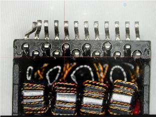
Telecentric lenses enable high-precision coplanarity inspection of electronic component leads
Achieving high-precision coplanarity inspection of electronic component leads is no easy feat. The advent of telecentric lenses has provided an effective solution to this challenge....
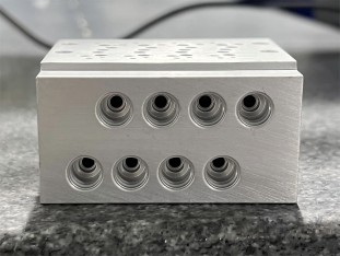
Telecentric lenses overcome challenges in deep hole/groove inspection
Inspecting deep holes (such as blind holes and through holes in mechanical parts) and grooves (such as retaining slots in electronic components and precision component channels) presents challenges......
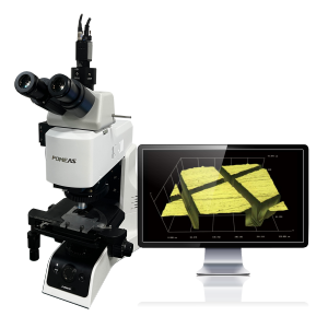
How to Tackle Surface Topography Analysis Challenges?
POMEAS Super Depth-of-Field Autofocus Microscope redefines surface topography inspection standards with its exceptional image processing capabilities and intelligent motorized control system....
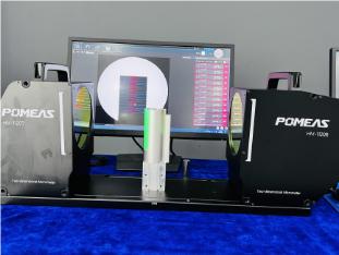
Ultra-Wide-Field Telecentric Measurement System | Precisely Captures Minor Wear on Metal Round Tubes
The HM-1120 telecentric measurement system with an ultra-wide field of view serves as the core inspection equipment, achieving 1.5μm precision to capture minute dimensional variations and ensure pr......
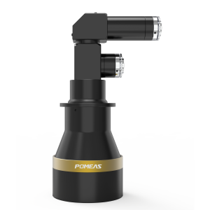
Application example of double telecentric lens: Watch inspection
The double telecentric lens effectively eliminates this interference, clearly revealing minor scratches, stains, and other imperfections on the glass surface, ensuring that every watch glass meets ......
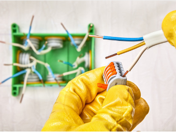
Telecentric Measurement System for Terminal Wire Spacing Inspection
The HM Series Telecentric Measurement System uses machine vision technology to achieve non-contact, high-precision, high-speed detection of terminal wire spacing....
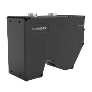
What are some typical applications of line laser profile sensors in industrial automation?
Line laser profile sensors have become a key technology in the field of industrial automation thanks to their high-precision 3D shape reconstruction capabilities and millisecond-level detection spe......
Product recommendation
TECHNICAL SOLUTION
MORE+You may also be interested in the following information
FREE CONSULTING SERVICE
Let’s help you to find the right solution for your project!

- APPICATION CASE
- RESOURCE CENTER
- DOWNLOAD CENTER
SOLUTIONS SUPPORT
- ZOOM LENS SELECTION TOOL
- TELECENTRIC LENS SELECTION TOOL
- FA LENS SELECTION TOOL
- ZOOM RATIO TABLE
- CERTIFIED MODEL
SELECTION TOOL
- WHY POMEAS
- FAQ
- PRIVACY POLICY
- TERMS OF USE
- DELIVERY & RETURN POLICY
CUSTOMER CARE
 ADDRESS
Add.:No.68, Chongwei Road, Baizhoubian, East district, Dongguan, China, 523000
CONTACT
 Tel:+ 86-0769-2266 0867
 Fax:+ 86-0769-2266 0867
 E-mail:marketing@pomeas.com

Wechat QR code




 ASK POMEAS
  PRICE INQUIRY
  REQUEST DEMO/TEST
  FREE TRIAL UNIT
  ACCURATE SELECTION