


Laser focus microscope system for inspection of semiconductor parts
Semiconductor parts play a pivotal role in modern industry and are widely used in electronic products, communication equipment, medical devices and many other fields. With the continuous development of science and technology, the performance and quality requirements for semiconductor parts are getting higher and higher. Therefore, how to accurately and efficiently detect semiconductor parts has become an urgent problem. As an advanced detection means, laser focusing microscope system has unique advantages, which can effectively solve the difficulties of semiconductor parts detection.
The difficulties in testing semiconductor parts are mainly in the following areas:

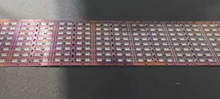
1: Semiconductor parts have complex structures and tiny dimensions, making it difficult for traditional inspection methods to accurately identify their internal structures and defects.
2: The manufacturing process of semiconductor parts is extremely demanding, and any tiny defects may affect their performance, so high-precision inspection means are needed.
3: The inspection process of semiconductor parts needs to be fast and accurate to meet the needs of mass production.
Detection Program:
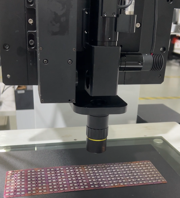
The laser focusing microscope system is designed to address these difficulties. It utilizes a laser beam as the illumination light source to magnify semiconductor parts at a high magnification rate through the microscope head, thus clearly showing the internal structure and defects of the parts. At the same time, the laser focusing microscope system is equipped with an auto-focusing function, which can quickly find the optimal observation position and greatly improve the inspection efficiency.
Laser focus microscopy system has many advantages in the inspection of semiconductor parts:
1, high-precision detection: laser focusing microscope system can achieve micron-level detection accuracy, accurately identifying small defects and structural changes within the semiconductor parts.
2, non-contact detection: laser focusing microscope system using non-contact detection, avoiding the traditional detection methods may introduce pollution and damage, to ensure the integrity of the semiconductor parts.
3, rapid detection: laser focusing microscope system has a fast auto-focus function, can complete a large number of semiconductor parts in a short period of time, to meet the needs of mass production.
4, visualization of inspection results: laser focusing microscope system can be the results of inspection in the form of images or video display, making the inspection process more intuitive, easy to understand.
Detection results:

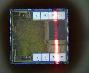
As an advanced inspection method, laser focusing microscope system has a broad application prospect in the field of semiconductor parts inspection. With the continuous progress and improvement of the technology, it is believed that the laser focusing microscope system will play an increasingly important role in the field of semiconductor parts inspection, and make a positive contribution to the promotion of the semiconductor industry's sustainable development.
Product recommendation
TECHNICAL SOLUTION
MORE+You may also be interested in the following information
FREE CONSULTING SERVICE
Let’s help you to find the right solution for your project!

 ASK POMEAS
  PRICE INQUIRY
  REQUEST DEMO/TEST
  FREE TRIAL UNIT
  ACCURATE SELECTION
 - APPICATION CASE
- RESOURCE CENTER
- DOWNLOAD CENTER
SOLUTIONS SUPPORT
- ZOOM LENS SELECTION TOOL
- TELECENTRIC LENS SELECTION TOOL
- FA LENS SELECTION TOOL
- ZOOM RATIO TABLE
- CERTIFIED MODEL
SELECTION TOOL
- WHY POMEAS
- FAQ
- PRIVACY POLICY
- TERMS OF USE
- DELIVERY & RETURN POLICY
CUSTOMER CARE
 ADDRESS
Add.:No.68, Yongwei Road, Baizhoubian, Dongcheng District, Dongguan, China,523000
CONTACT
 Tel:+ 86-0769-2266 0867
 Fax:+ 86-0769-2266 0867
 E-mail:marketing@pomeas.com

Wechat QR code
Software Copyright :2021SR0176001 抄袭必究, 技术支持:誉新源科技