


PCB ceramic substrate vision inspection is an important technology in the field of electronics manufacturing, which utilizes advanced machine vision systems for accurate and efficient inspection of ceramic substrates. Among them, Focus laser autofocus inspection system plays a vital role.

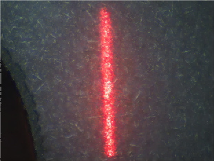
The Focus laser autofocus microscope utilizes a laser beam to scan a PCB ceramic substrate. First, the system emits a laser beam to the surface of the ceramic substrate, and some of the light is reflected when the laser touches the surface of the substrate. The system can accurately calculate the distance between the laser and the surface of the ceramic substrate by measuring the time difference between when the laser is emitted and when it receives the reflected light, and by combining this with the speed of light. This distance information is critical in determining the focus position of the lens, ensuring that the inspection system acquires a clear, accurate image.
After acquiring the images, the machine vision system will further process and analyze these images. By shooting the surface of the ceramic substrate with a high-resolution camera and using image processing algorithms to refine the analysis and processing of the image, it can realize the detection and analysis of the ceramic substrate surface defects, color difference, size, shape and other key parameters. Compared with traditional inspection methods, machine vision technology has higher inspection accuracy and efficiency, can greatly shorten the inspection time and reduce errors caused by human factors.
The Focus laser autofocus inspection system also has the ability to adaptively adjust the focus. Since the surface of a ceramic substrate may have different height and bump variations, the autofocus feature ensures that a clear image can be obtained at any position, thus increasing the accuracy and reliability of the inspection.

The POMEAS Focus laser autofocus inspection system plays a key role in the visual inspection of PCB ceramic substrates. It not only realizes high-precision and high-efficiency inspection, but also has the ability to adaptively adjust the focus to ensure accurate inspection results in any situation.
Product recommendation
TECHNICAL SOLUTION
MORE+You may also be interested in the following information
FREE CONSULTING SERVICE
Let’s help you to find the right solution for your project!

 ASK POMEAS
  PRICE INQUIRY
  REQUEST DEMO/TEST
  FREE TRIAL UNIT
  ACCURATE SELECTION
 - APPICATION CASE
- RESOURCE CENTER
- DOWNLOAD CENTER
SOLUTIONS SUPPORT
- ZOOM LENS SELECTION TOOL
- TELECENTRIC LENS SELECTION TOOL
- FA LENS SELECTION TOOL
- ZOOM RATIO TABLE
- CERTIFIED MODEL
SELECTION TOOL
- WHY POMEAS
- FAQ
- PRIVACY POLICY
- TERMS OF USE
- DELIVERY & RETURN POLICY
CUSTOMER CARE
 ADDRESS
Add.:No.68, Yongwei Road, Baizhoubian, Dongcheng District, Dongguan, China,523000
CONTACT
 Tel:+ 86-0769-2266 0867
 Fax:+ 86-0769-2266 0867
 E-mail:marketing@pomeas.com

Wechat QR code
Software Copyright :2021SR0176001 抄袭必究, 技术支持:誉新源科技