


Spectral Confocal Displacement Sensors For Precision Inspection Of Semiconductor Wafers!
With the development of the semiconductor industry and the advancement of the manufacturing process, the precision requirements for wafer manufacturing are getting higher and higher. In order to avoid defective wafers flowing into the subsequent process, it is necessary to do a good job of strict inspection. Pomeas, as a machine vision sensor device and solution provider, can provide effective assistance for wafer precision measurement!
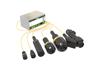
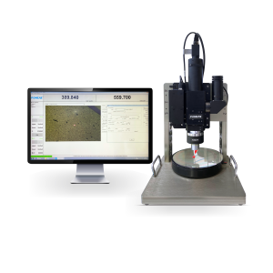
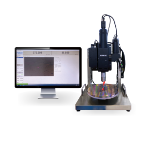
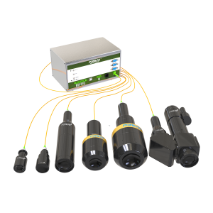
The PMS-8000SERIES spectral confocal displacement sensor is a non-contact displacement sensor that is independent of material and work form, and has a large measuring angle with nanometer accuracy. For wafer inspection, it is capable of using specular reflected light for measurement, and can also quickly visualise wafer surface data by adjusting the 3D view, thus obtaining high-quality three-dimensional surface topography data of the wafer and completing precision inspection. Compared with traditional measurement methods, spectral confocal sensors have obvious advantages such as high speed, high accuracy and high adaptability.
Spectral confocal displacement sensor in the semiconductor wafer inspection applications:
1. Thickness measurement: spectral confocal displacement sensors can achieve high-precision wafer thickness measurement to ensure the flatness of the wafer and manufacturing quality.
2. Accurate measurement of the roughness of the wafer surface to ensure that the surface quality meets the requirements.
3. Dimensional consistency measurement: Spectral confocal displacement sensors are capable of measuring wafers in multiple positions to ensure the consistency of wafer dimensions.
4. Wafer height measurement: through the spectral confocal displacement sensor, the position of the wafer at different depths can be accurately measured to ensure the flatness of the wafer.
As an advanced measurement technology, spectral confocal displacement sensor plays an increasingly important role in semiconductor wafer precision inspection. Through high-precision non-contact measurement, they are able to meet a variety of complex measurement needs and improve production efficiency and product quality.
Product recommendation
TECHNICAL SOLUTION
MORE+You may also be interested in the following information

Line Laser Displacement Sensor

FREE CONSULTING SERVICE
Let’s help you to find the right solution for your project!

 ASK POMEAS
  PRICE INQUIRY
  REQUEST DEMO/TEST
  FREE TRIAL UNIT
  ACCURATE SELECTION
 - APPICATION CASE
- RESOURCE CENTER
- DOWNLOAD CENTER
SOLUTIONS SUPPORT
- ZOOM LENS SELECTION TOOL
- TELECENTRIC LENS SELECTION TOOL
- FA LENS SELECTION TOOL
- ZOOM RATIO TABLE
- CERTIFIED MODEL
SELECTION TOOL
- WHY POMEAS
- FAQ
- PRIVACY POLICY
- TERMS OF USE
- DELIVERY & RETURN POLICY
CUSTOMER CARE
 ADDRESS
Add.:No.68, Chongwei Road, Baizhoubian, East district, Dongguan, China, 523000
CONTACT
 Tel:+ 86-0769-2266 0867
 Fax:+ 86-0769-2266 0867
 E-mail:marketing@pomeas.com

Wechat QR code
Software Copyright :2021SR0176001 抄袭必究, 技术支持:誉新源科技