


September Optics Expo Exhibits | WLI1000 3D White-Light Interferometric Profiler
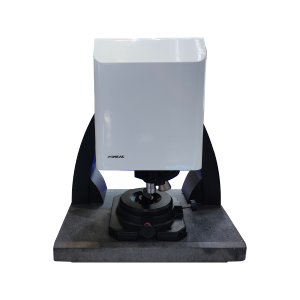
In the precision quality inspection processes of semiconductor manufacturing and micro/nanofabrication, many people have encountered the following challenges: contact-based measurement can easily scratch soft samples; conventional optical equipment cannot accurately measure ultra-smooth surfaces; and frequent switching between multiple devices is required for workpieces with different surface roughness levels, resulting in consistently low inspection efficiency. The WLI1000 3D White-Light Interferometric Profiler, showcased at Booth 1A75 at the Shenzhen Optics Fair, is specifically designed to address these industry pain points. A single solution can cover all precision inspection needs across the entire spectrum—from laboratory R&D to mass production on the shop floor.

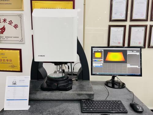
Nanoscale Non-Contact Measurement: Ensuring the Minimum Precision Threshold in Micro- and Nanoscale Processes
In many high-end manufacturing scenarios, even a height error of 0.5 nm can directly result in the entire batch of products being scrapped. This profilometer features a vertical resolution of less than 0.2 nm and a surface roughness repeatability consistently maintained at 0.01 nm. It employs non-contact measurement throughout the process, ensuring no surface damage to photoresists, flexible films, or polished soft components. It is fully suited for inspection scenarios—such as semiconductor wafers and MEMS devices—that demand extremely high surface integrity.
One system covers all types of surfaces, eliminating the need to switch instruments frequently
There’s no longer a need to prepare multiple inspection devices for different workpieces. Equipped with four measurement modes—PSI, VSI, ultra-deep depth of field, and brightfield—it precisely adapts to everything from ultra-smooth optically polished surfaces to rough workpieces with steep-angled walls. It also supports automatic image stitching for a wide field of view, enabling full-morphology inspection of large-area samples in a single pass and eliminating the tedious process of manual alignment.
Completes a single test in 5 seconds; compatible with materials of all reflectivity levels
In quality inspection processes on production lines where timing is of the essence, efficiency equals production capacity. Its PSI mode completes a single measurement in less than 5 seconds and supports inspection of workpieces with reflectance ranging from 0.1% to 100%. Whether dealing with highly reflective metallic surfaces or low-reflectance matte new materials, it quickly delivers stable and reliable measurement results, keeping pace with the inspection rhythm of mass production lines.
Comprehensive data analysis with one-click generation of customized reports
The comprehensive analysis software included covers the entire workflow—from 3D topography reconstruction and roughness calculation to step height measurement and 2D dimension annotation. It allows for the direct export of point cloud data and high-resolution topography images, and can generate customized reports based on quality inspection requirements across various industries. This eliminates the need for time-consuming manual data processing and enables inspection results to be directly integrated into the process optimization phase.
Designed for both laboratory and workshop environments, with flexible hardware configurations
The system is equipped with an electric XY stage and offers a wide selection of objectives. Combined with a long-travel Z-axis scanning mechanism, it not only meets the cutting-edge material analysis needs of universities and research institutions but can also be installed directly on the factory floor to perform batch appearance and dimensional quality inspections on workpieces such as automotive parts, mobile phone structural components, and watch hardware.
TECHNICAL SOLUTION
MORE+You may also be interested in the following information
FREE CONSULTING SERVICE
Let’s help you to find the right solution for your project!
 ASK POMEAS
  PRICE INQUIRY
  REQUEST DEMO/TEST
  FREE TRIAL UNIT
  ACCURATE SELECTION
- APPICATION CASE
- RESOURCE CENTER
- DOWNLOAD CENTER
SOLUTIONS SUPPORT
- ZOOM LENS SELECTION TOOL
- TELECENTRIC LENS SELECTION TOOL
- FA LENS SELECTION TOOL
- ZOOM RATIO TABLE
- CERTIFIED MODEL
SELECTION TOOL
- WHY POMEAS
- FAQ
- PRIVACY POLICY
- TERMS OF USE
- DELIVERY & RETURN POLICY
CUSTOMER CARE
 ADDRESS
Add.:No.68, Yongwei Road, Baizhoubian, Dongcheng District, Dongguan, China,523000
CONTACT
 Tel:+ 86-0769-2266 0867
 Fax:+ 86-0769-2266 0867
 E-mail:marketing@pomeas.com

Wechat QR code

Software Copyright :2021SR0176001 抄袭必究, 技术支持:誉新源科技