


What are the typical applications of spectral confocal displacement sensors?
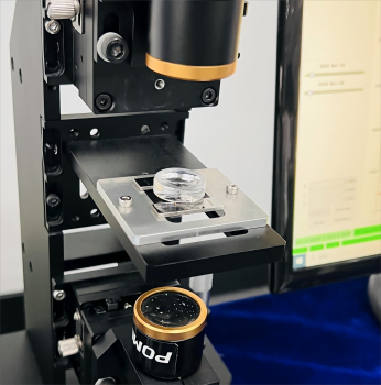
In today’s rapidly evolving landscape of precision manufacturing and automated inspection, achieving non-contact, high-precision measurements at the micrometer and even nanometer scales has become a common challenge across many industries. Spectral confocal displacement sensors are the key solution to this challenge.

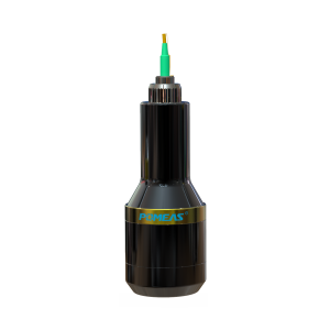
Principle of Spectral Confocal Displacement Sensors
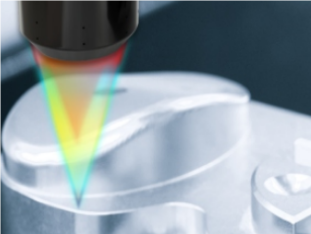
1. Coaxial measurement with no shadow obstruction: The optical path aligns with the measurement axis, allowing access to narrow spaces, deep holes, and other confined areas.
2. Exceptional material adaptability: It provides stable measurements on a wide range of surfaces—from highly reflective mirrors and transparent glass to rough black surfaces—without the need for recalibration.
3. Ultra-high resolution and linearity: Achieves nanometer-level resolution with a measurement spot size of just a few micrometers, making it ideal for micro-contour scanning. It is precisely these advantages that make it an indispensable measurement tool in the following scenarios.
Applications of Spectral Confocal Displacement Sensors

1. Smart Manufacturing and Automated Online Inspection
- Full inspection of precision component dimensions: such as the flatness of mobile phone mid-frames, the inner and outer diameters of bearings, and the height of connector terminals. Its high-speed sampling capability enables online 100% inspection at tens of thousands of points per second, eliminating the need for sampling.
- Dispensing and coating stations: Real-time measurement of adhesive path width, thickness, and wet film thickness, with closed-loop feedback for parameter adjustment to reduce defective products.
- Robotic Alignment and Positioning: Sensors integrated at the end effector of the robotic arm perform high-precision gap measurement and posture calibration prior to gripping and assembly, making it particularly suitable for handling mirror-finished or transparent workpieces.
2. Semiconductor and Electronic Components Industry

- Wafer Inspection: Measures wafer warpage, total thickness variation (TTV), and the thickness of transparent films such as oxide layers and photoresists, all without contact to prevent scratches.
- Advanced Packaging and Bonding: Measures chip height and bond pad coplanarity in chip stacking to ensure the reliability of wire bonding and flip-chip bonding.
- Lithography Systems and Precision Stages: Used for stage positioning feedback and nanometer-level gap control between the objective lens and the wafer, serving as a critical safeguard for the lithography process.
3. Glass and Transparent Materials Processing

- Consumer Electronics Glass: Contour scanning of 2.5D/3D curved glass for smartphone covers and automotive displays; measurement of edge radius and hole depth; and inspection of total thickness and air gaps after multi-layer glass lamination.
- Optical Components: Data on lens center thickness, lens spacing, and aspheric surface profiles can be rapidly acquired both before and after polishing.
- Flat-Panel Display Industry: Online monitoring of LCD/OLED panel substrate glass thickness, thin-film transistor layer thickness, and liquid crystal cell gaps to ensure display consistency.
4. Metal and Hard Materials Machining

- Precision Grinding and Cutting: Monitoring of tool wear, measurement of workpiece surface roughness and micro-profile, with the capability to be integrated into machine tools online without being affected by coolant interference.
- New Energy Battery Components: Parameters critical to battery safety—such as electrode thickness, explosion-proof valve groove depth, and busbar weld penetration profiles—can all be reliably detected.
- Additive Manufacturing (3D Printing): Real-time monitoring of layer-by-layer powder bed thickness and cladding layer morphology enables closed-loop control, improving print quality and yield rates.
5. Special Applications in Various Automated Inspection Processes

- Micro-holes and deep grooves: Chamfering of micro-holes in fuel injectors and the inner wall profiles of air film holes in turbine blades, measured using slender optical probes inserted into the features.
- Precision Medical Devices: Non-destructive testing of the inner and outer diameters of syringe barrels, the coating thickness of guide wires, and the surface profiles of artificial joints.
- Films and Flexible Materials: Measurement of the thickness and uniformity of lithium-ion battery separators and optical protective films, with real-time data acquisition during the unwinding process.
Product recommendation
TECHNICAL SOLUTION
MORE+You may also be interested in the following information
FREE CONSULTING SERVICE
Let’s help you to find the right solution for your project!

 ASK POMEAS
  PRICE INQUIRY
  REQUEST DEMO/TEST
  FREE TRIAL UNIT
  ACCURATE SELECTION
 - APPICATION CASE
- RESOURCE CENTER
- DOWNLOAD CENTER
SOLUTIONS SUPPORT
- ZOOM LENS SELECTION TOOL
- TELECENTRIC LENS SELECTION TOOL
- FA LENS SELECTION TOOL
- ZOOM RATIO TABLE
- CERTIFIED MODEL
SELECTION TOOL
- WHY POMEAS
- FAQ
- PRIVACY POLICY
- TERMS OF USE
- DELIVERY & RETURN POLICY
CUSTOMER CARE
 ADDRESS
Add.:No.68, Yongwei Road, Baizhoubian, Dongcheng District, Dongguan, China,523000
CONTACT
 Tel:+ 86-0769-2266 0867
 Fax:+ 86-0769-2266 0867
 E-mail:marketing@pomeas.com

Wechat QR code
Software Copyright :2021SR0176001 抄袭必究, 技术支持:誉新源科技