


Spectral Confocal Sensor: Non-contact Thickness Measurement of Transparent Silicon Wafers
Testing Background
In the semiconductor, photovoltaic, and precision electronics manufacturing sectors, silicon wafers serve as a core foundational material; their thickness consistency and precision directly impact the yield rates of subsequent processes and the performance of the final products. Traditional contact measurement methods, such as micrometers or coordinate measuring machines (CMMs), are widely used. However, when dealing with ultra-thin, fragile, and transparent silicon wafers, these methods carry risks of scratching, contamination, or deformation caused by probe pressure, making it difficult to meet modern demands for high-precision, high-efficiency non-destructive testing. Consequently, the industry has reached a consensus on the need for a non-contact, high-precision measurement solution capable of rapid response.

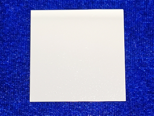
Test Object:The test specimens in this study were high-purity transparent silicon wafers. These wafers feature extremely high surface finish and excellent light transmittance, making them a key substrate material for the manufacture of high-end products such as integrated circuits and solar cells.
Challenges in Detection
1. Double-sided reflection interference: Because silicon wafers are highly transparent, traditional optical sensors receive reflected light from both the top and bottom surfaces of the wafer during measurement. This causes signal confusion, making it impossible to accurately identify the position of a single surface and, consequently, difficult to calculate the thickness precisely.
2. Non-contact requirement: Silicon wafers are fragile, and any physical contact may cause microcracks or contamination, affecting their electrical performance and mechanical strength; therefore, a completely non-contact measurement method must be employed.
3. High-precision requirements: As chip manufacturing processes continue to shrink, tolerance requirements for silicon wafer thickness have become increasingly stringent, typically needing to reach the micrometer (μm) or even submicrometer level. This places extremely high demands on the precision and stability of measurement equipment.
Testing Requirements
1. Accurately measure the distance from the top surface of the transparent silicon wafer to the probe (Distance 1);
2. Accurately measure the distance from the bottom surface of the transparent silicon wafer to the probe (Distance 2);
3. Based on the two distances above, accurately calculate the thickness of the silicon wafer (Thickness 1 = |Distance 1 - Distance 2|);
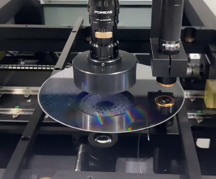
4. Measure 5 preset points on a single silicon wafer to evaluate its thickness uniformity.
Testing Protocol

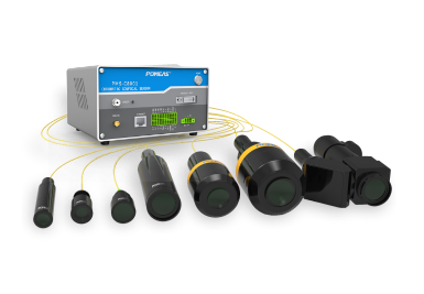
The solution employs POMEAS's proprietary SFS series point spectral confocal displacement sensor detection system. At the core of this system is the POMEAS SFS series spectral confocal sensor. Its operating principle involves using a white light source and a specialized dispersion lens assembly to focus light of different wavelengths at different heights along the optical axis. When the sensor is aligned with the target object, only light of specific wavelengths that are precisely in focus with the target surface is efficiently reflected and received by the spectrometer.
When measuring transparent silicon wafers, the sensor receives two distinct reflected peak signals simultaneously:
1. First peak: Corresponds to the position on the upper surface of the wafer; the system uses this to calculate distance 1.
2. Second peak: Corresponds to the position on the lower surface of the wafer; the system uses this to calculate distance 2.
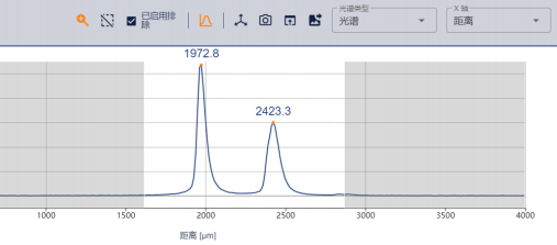
By processing these two peak signals in real time using an internal algorithm, the actual thickness of the silicon wafer (Thickness 1) can be calculated directly and accurately. The entire measurement process is completely non-contact and is not affected by the transparency of the silicon wafer.
Advantages of the Solution

1. Precise Identification of Multi-Layer Interfaces: Spectral confocal technology clearly distinguishes and captures reflection signals from the upper and lower surfaces of transparent objects, fundamentally resolving the signal interference issues encountered by traditional optical methods when measuring transparent materials and ensuring the accuracy of thickness calculations.
2. Fully Non-Contact, Non-Destructive Measurement: The measurement process requires no physical contact, completely eliminating the risk of scratching, contaminating, or deforming the wafer, and perfectly aligning with the non-destructive testing standards of high-end manufacturing.
3. High precision and stability: The SFS series sensors offer micron-level measurement accuracy and exceptional repeatability, meeting the stringent tolerance requirements for wafer thickness measurement. Measurement results are unaffected by changes in the surface color, inclination, or reflectivity of the measured object, ensuring stable and reliable data.
4. Compact, Efficient, and Easy to Integrate: Based on test results, a MINI controller paired with a 4mm probe fully meets measurement requirements. This combination is compact, responds quickly, and is easy to integrate into automated production lines, enabling 100% in-line inspection and effectively improving production efficiency and product yield.
Product recommendation
TECHNICAL SOLUTION
MORE+You may also be interested in the following information
FREE CONSULTING SERVICE
Let’s help you to find the right solution for your project!

 ASK POMEAS
  PRICE INQUIRY
  REQUEST DEMO/TEST
  FREE TRIAL UNIT
  ACCURATE SELECTION
 - APPICATION CASE
- RESOURCE CENTER
- DOWNLOAD CENTER
SOLUTIONS SUPPORT
- ZOOM LENS SELECTION TOOL
- TELECENTRIC LENS SELECTION TOOL
- FA LENS SELECTION TOOL
- ZOOM RATIO TABLE
- CERTIFIED MODEL
SELECTION TOOL
- WHY POMEAS
- FAQ
- PRIVACY POLICY
- TERMS OF USE
- DELIVERY & RETURN POLICY
CUSTOMER CARE
 ADDRESS
Add.:No.68, Yongwei Road, Baizhoubian, Dongcheng District, Dongguan, China,523000
CONTACT
 Tel:+ 86-0769-2266 0867
 Fax:+ 86-0769-2266 0867
 E-mail:marketing@pomeas.com

Wechat QR code
Software Copyright :2021SR0176001 抄袭必究, 技术支持:誉新源科技