


Applications of Image Dimension Measuring Instruments in Precision Manufacturing
In the competitive arena of precision manufacturing, micron-level accuracy determines the success or failure of products and the competitiveness of companies. Whether it’s the precision connectors in smartphones, the life-critical microcomponents in medical devices, or the precision valve cores in automotive engines, their dimensional tolerances are extremely stringent. Traditional manual caliper measurements or projection system inspections often fall short when dealing with high-volume production and intricate, microscopic structures—plagued by low efficiency, operator fatigue, and significant subjective errors, they have become a bottleneck in quality control.
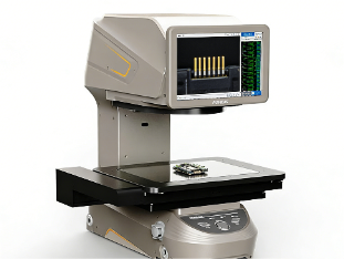
Today, image dimension measurement systems—as high-precision, non-contact optical measurement solutions—are rapidly becoming the “eyes” of modern precision manufacturing facilities. Their core principle involves using high-resolution industrial cameras and specialized optical lenses to magnify and capture images of the workpiece. Advanced image processing and algorithm software then automatically identify, extract, and calculate edge contours, thereby quickly obtaining various dimensional data on a two-dimensional plane.

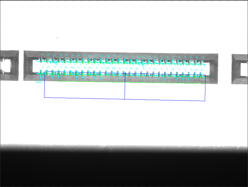
In the 3C electronics industry, image-based dimensional measurement systems prove invaluable. Take, for example, the shielding cover or FPC flex circuit on a mobile phone motherboard, which is densely populated with alignment holes, tiny pads, and minute gaps. Manual measurement is not only time-consuming but also highly prone to errors. In contrast, an image measurement system equipped with an automatic stage and programmable software can rapidly scan the entire board, automatically measuring and evaluating dozens or even hundreds of critical dimensions in a single pass. This enables 100% inspection, ensuring that every motherboard meets design specifications.
In the precision hardware and mold industry, contour accuracy, positional accuracy, and hole diameter are key metrics for stamped and injection-molded parts. With its powerful contour lighting, the imaging system clearly outlines the edges of workpieces, accurately capturing even subtle features such as radii and chamfers. For mass production requiring SPC (Statistical Process Control) analysis, the imaging system automatically records and analyzes data, monitoring the stability of the production process in real time and providing early warnings of potential quality drifts.
Furthermore, in highly demanding sectors such as semiconductors and medical devices, image-based dimensional measurement systems not only provide dimensional data but also utilize high-definition imaging capabilities to simultaneously detect surface defects—such as scratches, stains, and burrs—enabling a “multi-functional” approach. Take the industry-renowned Promis Measurement Technology as an example. Its image-based dimensional measurement solutions, through highly automated and intelligent design, help manufacturing enterprises upgrade quality control from experience-dependent “visual inspection” to data-driven “scientific decision-making.” This significantly enhances production efficiency and product consistency, firmly safeguarding the quality lifeline of precision manufacturing.
Product recommendation
TECHNICAL SOLUTION
MORE+You may also be interested in the following information
FREE CONSULTING SERVICE
Let’s help you to find the right solution for your project!

 ASK POMEAS
  PRICE INQUIRY
  REQUEST DEMO/TEST
  FREE TRIAL UNIT
  ACCURATE SELECTION
 - APPICATION CASE
- RESOURCE CENTER
- DOWNLOAD CENTER
SOLUTIONS SUPPORT
- ZOOM LENS SELECTION TOOL
- TELECENTRIC LENS SELECTION TOOL
- FA LENS SELECTION TOOL
- ZOOM RATIO TABLE
- CERTIFIED MODEL
SELECTION TOOL
- WHY POMEAS
- FAQ
- PRIVACY POLICY
- TERMS OF USE
- DELIVERY & RETURN POLICY
CUSTOMER CARE
 ADDRESS
Add.:No.68, Chongwei Road, Baizhoubian, East district, Dongguan, China, 523000
CONTACT
 Tel:+ 86-0769-2266 0867
 Fax:+ 86-0769-2266 0867
 E-mail:marketing@pomeas.com

Wechat QR code
Software Copyright :2021SR0176001 抄袭必究, 技术支持:誉新源科技