


Laser AF System Enables Precision Inspection of Semiconductors/Electronics
In precision manufacturing fields such as semiconductor wafer dust detection and solder joint inspection of electronic components, millisecond focusing delays can lead to defects being missed, and the slow manual or mechanical focusing of traditional microscopy systems has become a bottleneck that limits efficiency and accuracy. POMEAS laser autofocus microscope was born to revolutionize the accurate and real-time focusing ability, setting a new benchmark for high-precision microscopic observation.

Core Technology Advantage: The Perfect Fusion of Speed, Precision and Intelligence
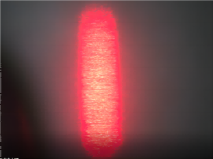
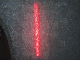
1. Laser instantaneous sensing, precise focus locking: The core of the system is equipped with a highly sensitive laser sensor, which is like equipping the microscope with an “intelligent eye”. With a focusing frequency of up to 5000 Hz, it continuously scans the height information of the sample surface at high speed and instantly captures the micron-level topography. Combined with advanced algorithms, no matter how complex the surface undulation is, it can be accurately locked within 0.4 seconds, bidding farewell to the time-consuming and uncertainty of repeated focus adjustments.

2. Intelligent real-time focusing for worry-free dynamic capture: POMEAS systems demonstrate excellent dynamic performance in the face of moving samples on the production line or small deformations caused by thermal expansion and contraction. 5000Hz refresh rate ensures that the focus is always “close” to the target, realizing true “zero” latency real-time focusing. "Real-time focusing with zero delay. Whether it's high-speed inspection on an automated production line or real-time monitoring of a precision welding process, the focus remains stable and details are visible.


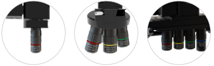
3. Multi-objective lens seamless cooperation, flexible application expansion: The system innovatively integrates the intelligent objective lens focusing motion module and objective lens mounting mechanism, which supports fast and accurate switching of APO (achromatic aberration) objective lenses with different magnification and different working distance. Combined with a Z-axis travel of ±15mm, the system can easily cope with diversified inspection needs from ultra-thin wafers to electronic components with a certain thickness, making it multi-purpose and multiplying its performance.
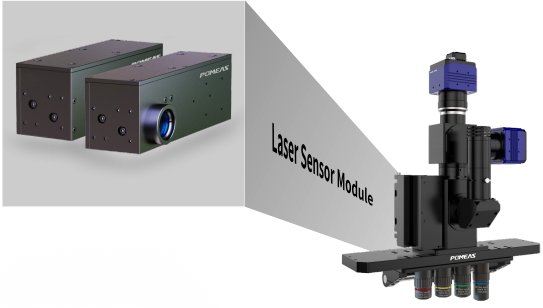
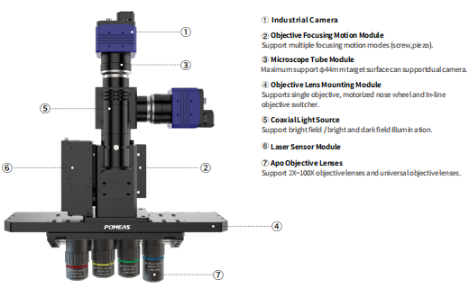
4. Precision collaboration of all modules: The system consists of industrial camera (high-definition imaging), microscope tube (stable optical path), light source system (optimized illumination), objective focusing motion module (fast and accurate Z-axis movement), laser sensor (core ranging), objective lens mounting mechanism (flexible switching), and APO objective lenses (excellent optical performance), which are the seven core components that collaborate to build a solid, reliable and high-performance observation platform.
Empowering high-precision industries: a double leap in efficiency and quality
-
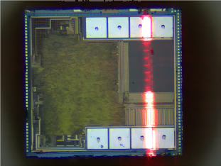
Semiconductor Wafer Manufacturing: In nano-scale wafer defect inspection, POMEAS system ensures that every frame of image is clear and sharp under high speed scanning with ultra-fast focusing and real-time focusing capability. Whether it is fine scratches, particle contamination or graphical defects, all can be accurately captured, significantly improving the inspection coverage and yield rate, and safeguarding the chip quality.
-
Precision Inspection of Electronic Components: Observation of critical quality points such as the curvature of wire bonding, solder ball morphology, and coplanarity of connector pins requires high stability. The system accurately locks onto the target area within 0.4 seconds and maintains the optimal focus in real time during subsequent inspections, clearly presenting micron-level details to ensure connection reliability and product performance.

POMEAS laser autofocus microscope is not only a technological innovation, but also a promise of efficiency and precision. It redefines the standard for high-precision microscopy, makes “instant locking” and “dynamic following” a reality, and empowers the semiconductor and electronics industries to gain insights into the microcosmic world and harness the future.
Product recommendation
TECHNICAL SOLUTION
MORE+You may also be interested in the following information
FREE CONSULTING SERVICE
Let’s help you to find the right solution for your project!

 ASK POMEAS
  PRICE INQUIRY
  REQUEST DEMO/TEST
  FREE TRIAL UNIT
  ACCURATE SELECTION
 - APPICATION CASE
- RESOURCE CENTER
- DOWNLOAD CENTER
SOLUTIONS SUPPORT
- ZOOM LENS SELECTION TOOL
- TELECENTRIC LENS SELECTION TOOL
- FA LENS SELECTION TOOL
- ZOOM RATIO TABLE
- CERTIFIED MODEL
SELECTION TOOL
- WHY POMEAS
- FAQ
- PRIVACY POLICY
- TERMS OF USE
- DELIVERY & RETURN POLICY
CUSTOMER CARE
 ADDRESS
Add.:No.68, Chongwei Road, Baizhoubian, East district, Dongguan, China, 523000
CONTACT
 Tel:+ 86-0769-2266 0867
 Fax:+ 86-0769-2266 0867
 E-mail:marketing@pomeas.com

Wechat QR code
Software Copyright :2021SR0176001 抄袭必究, 技术支持:誉新源科技