


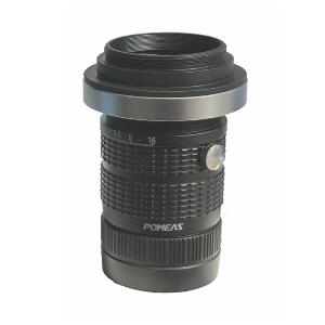
4K Line Scan Industrial Lens Series: High Speed High Precision Inspection Lens
With the rapid development of industrial automation and machine vision technology, high-precision and high-efficiency inspection equipment has become the core competitiveness to guarantee product quality. POMEAS LL4K line scan industrial lens series has become the ideal choice for semiconductor, display panel, new energy and other fields with its large target surface design, ultra-low aberration, anti-vibration and wide coverage of base magnification. With its large target surface design, ultra-low distortion, anti-vibration function and wide reference magnification coverage, the LL4K line scan industrial lens series has become the ideal choice for semiconductors, display panels, new energy, etc., providing one-stop solutions for high-speed and high-precision inspection scenes.

Large target surface design, covering multiple scenarios
LL4K series adopts φ32mm-φ82mm large target surface design, which can be adapted to a variety of sensor sizes, significantly improving the effective imaging area and reducing the need for splicing, especially suitable for large-size wafers, LCD panels and other wide-area inspection scenarios. The combination of 7μm high resolution and <0.1% ultra-low distortion technology ensures that the image is maintained from the edge to the center. The combination of 7μm high resolution and <0.1% ultra-low distortion technology ensures that the image maintains high definition and geometric consistency from the edge to the center, providing a reliable data base for micron-level defect identification.
High speed and stability for demanding production lines
For high-speed production line needs, this series supports 0.015X-3.5X reference magnification flexible adjustment, covering the whole process of inspection from macroscopic positioning to microscopic detail analysis. Its anti-vibration design and optimized conjugate distance (up to 2182mm) effectively suppresses Its anti-vibration design and optimized conjugate distance (up to 2182mm) effectively suppresses mechanical vibration interference and maintains image stability even in high-speed motion, which meets the high real-time requirements of semiconductor wafers, OLED evaporation and plating processes, and other applications.
Intelligent Integration to Reduce Deployment Costs
The modular design supports seamless integration with coaxial light source and industrial cameras, and provides multiple interface options such as M42/M72/F port to simplify the system construction process. With POMEAS self-developed vision algorithms, it can realize automatic classification of defects, size measurement and other functions, which significantly reduces the maintenance and upgrade costs.
The 4K line scan lens can be applied in inspection solutions such as semiconductor wafer defect inspection; OLED front-end process inspection; LCD/TFT surface defect analysis.
Product recommendation
TECHNICAL SOLUTION
MORE+You may also be interested in the following information
FREE CONSULTING SERVICE
Let’s help you to find the right solution for your project!

 ASK POMEAS
  PRICE INQUIRY
  REQUEST DEMO/TEST
  FREE TRIAL UNIT
  ACCURATE SELECTION
 - APPICATION CASE
- RESOURCE CENTER
- DOWNLOAD CENTER
SOLUTIONS SUPPORT
- ZOOM LENS SELECTION TOOL
- TELECENTRIC LENS SELECTION TOOL
- FA LENS SELECTION TOOL
- ZOOM RATIO TABLE
- CERTIFIED MODEL
SELECTION TOOL
- WHY POMEAS
- FAQ
- PRIVACY POLICY
- TERMS OF USE
- DELIVERY & RETURN POLICY
CUSTOMER CARE
 ADDRESS
Add.:No.68, Chongwei Road, Baizhoubian, East district, Dongguan, China, 523000
CONTACT
 Tel:+ 86-0769-2266 0867
 Fax:+ 86-0769-2266 0867
 E-mail:marketing@pomeas.com

Wechat QR code
Software Copyright :2021SR0176001 抄袭必究, 技术支持:誉新源科技