


In the field of semiconductor manufacturing, wafer inspection is the core link to ensure product quality and yield. With the process node to 3nm or even more advanced process, the detection accuracy requirements have broken through the micron level, and the complexity of the wafer manufacturing environment further exacerbated the difficulty of equipment selection. Industrial lens as a visual inspection system “eyes”, its performance directly determines the accuracy and efficiency of defect recognition.

A、Core Challenges in Semiconductor Wafer Inspection

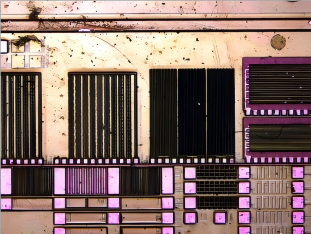
1. high-precision imaging needs: wafer surface defect size may be less than 0.1μm, requiring the lens resolution of 10 million pixels, and the distortion rate is less than 0.1%.
2. multi-spectral compatibility: different inspection tasks need to match specific wavelengths , the lens needs to support a wide spectral range .
B、Industrial Lens Selection Elements

1. Optical performance parameters
(1) resolution and pixel matching: select the lens magnification according to the camera sensor size to ensure that the lens MTF curve is still higher than 30% at the Nyquist frequency
(2) aberration correction capability: give priority to compound achromatic aberration (APO) design lenses to eliminate the effects of chromatic aberration and spherical aberration on the edge imaging quality, and safeguard the uniformity of the full field of view.
(3) working distance and depth of field: combined with the detection of object distance (such as wafer and lens distance) to calculate the depth of field range, to avoid imaging blurring due to mechanical vibration.
2. Mechanical structure and protection class
(1) sealing and Material: adopting full metal body with double O-ring sealing design, it meets IP67 protection level and prevents water vapor/dust intrusion.
(2) interface compatibility: support C-Mount, F-Mount and other industrial standard interfaces, easy to integrate with existing testing equipment.
(3) focusing and locking mechanism: equipped with locking ring and scale marking to prevent vibration-induced focus shift.
In the field of semiconductor wafer inspection, industrial lens selection has evolved from a single optical parameter competition to environmental adaptability, system integration and intelligent competition.
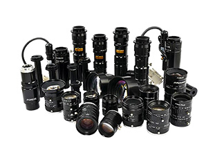
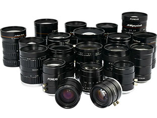
Product recommendation
TECHNICAL SOLUTION
MORE+You may also be interested in the following information
FREE CONSULTING SERVICE
Let’s help you to find the right solution for your project!

 ASK POMEAS
  PRICE INQUIRY
  REQUEST DEMO/TEST
  FREE TRIAL UNIT
  ACCURATE SELECTION
 - APPICATION CASE
- RESOURCE CENTER
- DOWNLOAD CENTER
SOLUTIONS SUPPORT
- ZOOM LENS SELECTION TOOL
- TELECENTRIC LENS SELECTION TOOL
- FA LENS SELECTION TOOL
- ZOOM RATIO TABLE
- CERTIFIED MODEL
SELECTION TOOL
- WHY POMEAS
- FAQ
- PRIVACY POLICY
- TERMS OF USE
- DELIVERY & RETURN POLICY
CUSTOMER CARE
 ADDRESS
Add.:No.68, Chongwei Road, Baizhoubian, East district, Dongguan, China, 523000
CONTACT
 Tel:+ 86-0769-2266 0867
 Fax:+ 86-0769-2266 0867
 E-mail:marketing@pomeas.com

Wechat QR code
Software Copyright :2021SR0176001 抄袭必究, 技术支持:誉新源科技