


In the field of industrial manufacturing, three-dimensional contour inspection technology is upgraded from the quality control “auxiliary tool” to the core engine of the whole chain efficiency. From the car body surface accuracy to the semiconductor wafer microscopic morphology, from the medical device surface defects to the 3C electronic assembly gap, three-dimensional contour data has become a key code to crack the production bottleneck, optimize the process.
Industry Cases
1、In the field of injection molding, through the three-dimensional profile analysis of the mold surface, the optimization interval of injection pressure, holding time and other parameters can be deduced in reverse direction;

2、In 3C electronics, 3D contour data can drive robotic arms for dynamic error compensation;

3、In the medical device industry, CT scanning and 3D reconstruction technology can accurately locate 0.03mm cracks inside implants;
4、The 3D data is deeply integrated with the MES system, which can build a digital mirror of the whole life cycle of the product.
3D Measurement Program
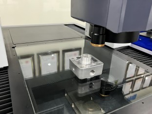
1. Line Laser Scanning Sensor Inspection Program

For dynamic inspection scenarios such as automotive parts, 3C electronics, etc., it adopts the combination of high-precision linear slide table and submicron line laser sensor. The supporting MetX measurement software has a built-in AI denoising algorithm, which can automatically identify product feature points and generate inspection reports. In new energy vehicle battery tray inspection, the solution compresses the inspection efficiency from 25 minutes/piece to 75 seconds/piece, with a repeatable positioning accuracy of ±0.025mm, and supports the output of surface contour deviation color gradient map.
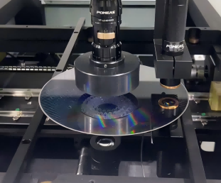
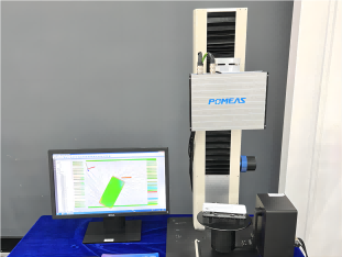
2. MetX Multi-sensor Measurement System

The system supports spectral confocal, line laser, point laser and other 6 types of sensors plug and play, through the five-axis linkage motion platform to realize the composite dimension measurement. In the field of semiconductor packaging, the system can simultaneously complete the wafer warpage, pin coplanarity, solder ball diameter and other 12 parameters, compared with the traditional equipment to improve the efficiency of 10 times, the measurement accuracy exceeded ± 0.3 μm. Its modular design to support the customization of the sensor combination, to adapt to the needs of the inspection of micro-components to large-scale workpieces.
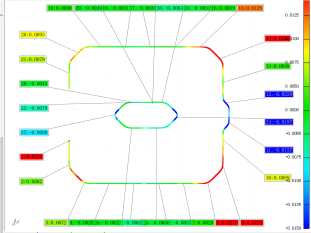
3. Spot Spectrum Scanning Measurement Equipment

Adopting the patented profiling scanning algorithm, it can automatically plan the inspection path for complex surfaces such as automotive glass and optical lenses. In the production line of high-end automotive window suppliers, the equipment realizes 3D contour deviation color gradation map output, which improves the inspection efficiency by 18 times compared with contact measurement and avoids surface scratches that may be caused by traditional fixtures. The non-contact measurement feature is especially suitable for the inspection of fragile materials such as medical implants and precision ceramics.
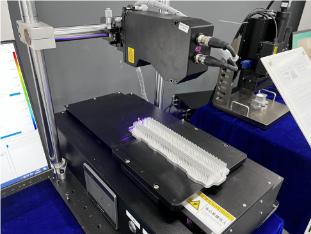
4. 3D Structured Light Scanning Solution

Through dynamic stripe projection and GPU-accelerated computation, full-size inspection of small and medium-sized workpieces, such as cell phone middle frames, is completed within 3 seconds. In the production line of smart wearable devices, the solution realizes a repeatability of 0.015mm, and reduces the defective rate of assembly gap from 2.2% to 0.1% through point cloud comparison technology. Its ability to resist ambient light interference enables it to operate stably in the bright light environment of the production line.
Product recommendation
TECHNICAL SOLUTION
MORE+You may also be interested in the following information
FREE CONSULTING SERVICE
Let’s help you to find the right solution for your project!

 ASK POMEAS
  PRICE INQUIRY
  REQUEST DEMO/TEST
  FREE TRIAL UNIT
  ACCURATE SELECTION
 - APPICATION CASE
- RESOURCE CENTER
- DOWNLOAD CENTER
SOLUTIONS SUPPORT
- ZOOM LENS SELECTION TOOL
- TELECENTRIC LENS SELECTION TOOL
- FA LENS SELECTION TOOL
- ZOOM RATIO TABLE
- CERTIFIED MODEL
SELECTION TOOL
- WHY POMEAS
- FAQ
- PRIVACY POLICY
- TERMS OF USE
- DELIVERY & RETURN POLICY
CUSTOMER CARE
 ADDRESS
Add.:No.68, Chongwei Road, Baizhoubian, East district, Dongguan, China, 523000
CONTACT
 Tel:+ 86-0769-2266 0867
 Fax:+ 86-0769-2266 0867
 E-mail:marketing@pomeas.com

Wechat QR code
Software Copyright :2021SR0176001 抄袭必究, 技术支持:誉新源科技