


Integrated solution for micro-observation and precision measurement of PCB
1. High-precision autofocus tool microscope core function highlights
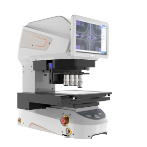
(1) Realize full-automatic focusing technology: one-key intelligent focusing, eliminating manual operation errors, greatly improving PCB micro-observation efficiency, especially suitable for multilayer board microvia, line defects detection and other precision scenarios.
(2) 0.1μm ultra-high precision measurement: equipped with a nano-scale mobile platform, the resolution reaches the submicron level, which easily realizes the precise quantitative analysis of key parameters such as solder joint size and line width spacing.
(3) Integrated design: Fusion of microscopic imaging and metrology functions, support for 2D/3D composite measurement, farewell to the traditional “observation-transfer-measurement” multi-device operation process.
2. Traditional tool microscope pain point breakthrough
(1) The traditional tool microscope relies on manual focusing, with low repetitive positioning accuracy (usually >1μm), making it difficult to meet the inspection needs of advanced processes such as HDI boards and chip packaging.
(2) Traditional tool microscopes do not have an automated platform, resulting in low measurement efficiency and poor data consistency, which can easily lead to blind spots in quality control.
(3) POMEAS high-precision auto-focus tool microscope ensures the traceability of the whole process data through closed-loop grating control system + AI image algorithm.
3. Typical application scenarios for PCBs

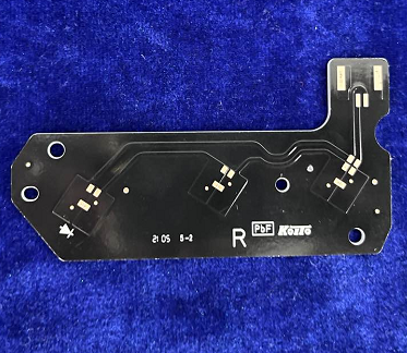
◼ High Density PCB Microvia Conductivity Inspection
◼ Deformation Stress Analysis of Flexible Circuit Boards
◼ Semiconductor package BGA solder ball 3D reconstruction
◼ SMT placement process quality control
TECHNICAL SOLUTION
MORE+You may also be interested in the following information
FREE CONSULTING SERVICE
Let’s help you to find the right solution for your project!

 ASK POMEAS
  PRICE INQUIRY
  REQUEST DEMO/TEST
  FREE TRIAL UNIT
  ACCURATE SELECTION
 - APPICATION CASE
- RESOURCE CENTER
- DOWNLOAD CENTER
SOLUTIONS SUPPORT
- ZOOM LENS SELECTION TOOL
- TELECENTRIC LENS SELECTION TOOL
- FA LENS SELECTION TOOL
- ZOOM RATIO TABLE
- CERTIFIED MODEL
SELECTION TOOL
- WHY POMEAS
- FAQ
- PRIVACY POLICY
- TERMS OF USE
- DELIVERY & RETURN POLICY
CUSTOMER CARE
 ADDRESS
Add.:No.68, Chongwei Road, Baizhoubian, East district, Dongguan, China, 523000
CONTACT
 Tel:+ 86-0769-2266 0867
 Fax:+ 86-0769-2266 0867
 E-mail:marketing@pomeas.com

Wechat QR code
Software Copyright :2021SR0176001 抄袭必究, 技术支持:誉新源科技