


In modern electronics manufacturing, chips and PCBs (printed circuit boards) are the core components of electronic devices. Their surface quality directly affects product performance and reliability. However, the surface structure of these precision components is complex, and traditional inspection methods are often difficult to meet the needs of high-precision and high-efficiency inspection. In recent years, a technology called “Spectral Confocal Sensor” has emerged as a powerful tool for chip and PCB surface inspection.
The working principle of a spectral confocal sensor can be simply understood as “touching an object with light”. It emits a beam of white light with a broad spectrum, which is focused on the surface of the object to be measured through a lens. As different wavelengths of light are focused at different heights, only the wavelengths that match the height of the surface being measured are reflected back, and by analyzing the wavelengths of the reflected light, the height information of the point being measured can be accurately calculated.
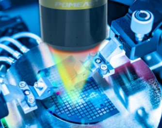
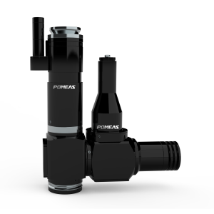
POMEAS Spectral Confocal Sensor SFS series is a typical representative of this technology. It has 7 different sizes of spectral probes, which can be adapted to different sizes and shapes of inspection needs. Together with the dedicated spectral control box and measurement software, the SFS series is able to quickly scan the surface of chips and PCBs and accurately reconstruct the three-dimensional profile of the DUT.

In practical applications, the SFS series of spectral probes have demonstrated strong performance:
1. High precision: axial resolution up to the nanometer level, able to detect the smallest defects on the surface of chips and PCBs.
2. High efficiency: non-contact measurement, tens of thousands of data points can be collected per second, greatly improving the detection efficiency.
3. Strong adaptability: able to measure a variety of material surfaces, including metals, ceramics, plastics, etc., to adapt to the complex production environment.
4. Intuitive display: the measurement software can real-time display of three-dimensional topography, easy to quickly determine the quality of the product.
In chip manufacturing, the SFS series can be used to detect key parameters such as wafer surface flatness and etching depth; in PCB production, it can accurately measure pad height, line width, etc. to ensure the reliability of circuit connections.
Product recommendation
TECHNICAL SOLUTION
MORE+You may also be interested in the following information
FREE CONSULTING SERVICE
Let’s help you to find the right solution for your project!

 ASK POMEAS
  PRICE INQUIRY
  REQUEST DEMO/TEST
  FREE TRIAL UNIT
  ACCURATE SELECTION
 - APPICATION CASE
- RESOURCE CENTER
- DOWNLOAD CENTER
SOLUTIONS SUPPORT
- ZOOM LENS SELECTION TOOL
- TELECENTRIC LENS SELECTION TOOL
- FA LENS SELECTION TOOL
- ZOOM RATIO TABLE
- CERTIFIED MODEL
SELECTION TOOL
- WHY POMEAS
- FAQ
- PRIVACY POLICY
- TERMS OF USE
- DELIVERY & RETURN POLICY
CUSTOMER CARE
 ADDRESS
Add.:No.68, Chongwei Road, Baizhoubian, East district, Dongguan, China, 523000
CONTACT
 Tel:+ 86-0769-2266 0867
 Fax:+ 86-0769-2266 0867
 E-mail:marketing@pomeas.com

Wechat QR code
Software Copyright :2021SR0176001 抄袭必究, 技术支持:誉新源科技