


Dual telecentric lenses: Semiconductor package solder ball diameter inspection accuracy jumps to 1μm
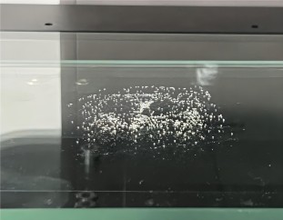
In the precision manufacturing field of semiconductor packaging, accurate detection of the diameter of the solder balls is crucial. The smallest deviation in the diameter of the solder ball may affect the performance and reliability of the entire semiconductor device. POMEAS has developed a dual telecentric lens, which has successfully improved the accuracy of tin ball diameter detection to 1μm, bringing a new technological breakthrough to the semiconductor packaging industry.

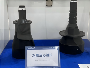
The double telecentric lens has unique optical characteristics. Its object-side telecentric optical path and image-side telecentric optical path effectively eliminate measurement errors caused by changes in object distance, ensuring stable acquisition of high-precision images at different working distances. This feature enables the dual telecentric lens to maintain excellent performance in complex semiconductor packaging production environments.

In semiconductor packaging, tin ball as a key component connecting the chip and the substrate, the precise control of its diameter is directly related to the quality of the electrical connection of the chip and the efficiency of signal transmission. Traditional inspection methods have certain limitations in terms of accuracy, making it difficult to meet the growing demand for high-precision inspection. POMEAS' dual telecentric lenses, with their excellent optical performance, can clearly capture the subtle contours of the solder balls, and through advanced image algorithms and processing technology, realize high-precision measurement of the diameter of the solder balls.

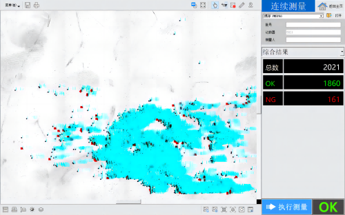
The increased detection accuracy of 1μm means that during the semiconductor packaging process, tin balls that meet the standards can be screened more accurately, reducing the rate of product defects due to deviations in the diameter of the balls. This not only helps to improve the overall quality of semiconductor devices, but also effectively reduces production costs and improves production efficiency.
Product recommendation
TECHNICAL SOLUTION
MORE+You may also be interested in the following information
FREE CONSULTING SERVICE
Let’s help you to find the right solution for your project!

 ASK POMEAS
  PRICE INQUIRY
  REQUEST DEMO/TEST
  FREE TRIAL UNIT
  ACCURATE SELECTION
 - APPICATION CASE
- RESOURCE CENTER
- DOWNLOAD CENTER
SOLUTIONS SUPPORT
- ZOOM LENS SELECTION TOOL
- TELECENTRIC LENS SELECTION TOOL
- FA LENS SELECTION TOOL
- ZOOM RATIO TABLE
- CERTIFIED MODEL
SELECTION TOOL
- WHY POMEAS
- FAQ
- PRIVACY POLICY
- TERMS OF USE
- DELIVERY & RETURN POLICY
CUSTOMER CARE
 ADDRESS
Add.:No.68, Chongwei Road, Baizhoubian, East district, Dongguan, China, 523000
CONTACT
 Tel:+ 86-0769-2266 0867
 Fax:+ 86-0769-2266 0867
 E-mail:marketing@pomeas.com

Wechat QR code
Software Copyright :2021SR0176001 抄袭必究, 技术支持:誉新源科技