


What lenses are needed to detect scratches on the surface of a chip?
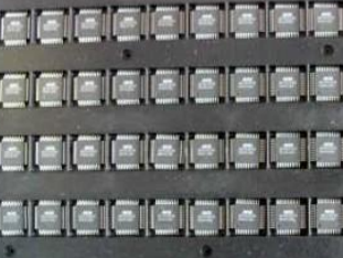
In today's rapid development of high technology, the quality of the chip, as a core component of electronic equipment, is directly related to the performance and reliability of the entire product. However, in the production and processing of chips, surface scratches and other minor defects are often difficult to avoid, these defects not only affect the aesthetics of the chip, but also may pose a potential threat to its function. Therefore, the use of high-precision and high-efficiency industrial lenses for chip surface scratch detection is particularly important. This article will discuss in depth in the field of chip inspection, how to choose the right industrial lens to accurately capture and identify these small defects, so as to ensure the excellence and stability of the chip quality.

Selection Recommendations
(1) Detection accuracy: according to the size of the chip surface scratches and detection accuracy requirements, select the appropriate lens magnification and resolution.
(2) Field of view: according to the size of the chip and the size of the detection area, select the appropriate lens field of view.
(3) Lens compatibility: Ensure that the selected lens is compatible with the camera, light source and other detection equipment interface and parameters.
(4) Lens performance: select a lens with good imaging quality, low distortion, high parallelism and large depth of field to ensure the accuracy and consistency of detection.
Q:Which lenses are suitable for chip appearance defect detection?
1. 4K zoom lens is characterized by large target surface and high resolution imaging, and the size of the field of view is improved compared with the traditional zoom lens, which can meet the requirements of high-precision inspection of chips.

Application: In chip visual inspection, 4K zoom lens can clearly and quickly identify the defects such as scratches, faults, missing pins and other defects on the chip. For example, POMEAS 4K zoom lens performs well in the detection of chip appearance defects, and its machine vision chip inspection program has the advantages of fast detection speed, high precision, and high detection efficiency compared with manual inspection.
2. High-resolution macro lenses usually have high magnification and resolution to capture minute details.

Application: In chip surface scratch inspection, high resolution macro lens can clearly show the tiny scratches and defects on the chip surface.
3. The telecentric lens is characterized by low distortion, high parallelism and large depth of field, which is suitable for accurate measurement and positioning of objects.

Application: In chip inspection, telecentric lenses can ensure the accuracy and consistency of measurement, especially when it is necessary to measure the length and width of scratches and other parameters are more suitable.
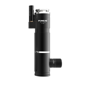
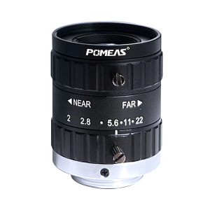
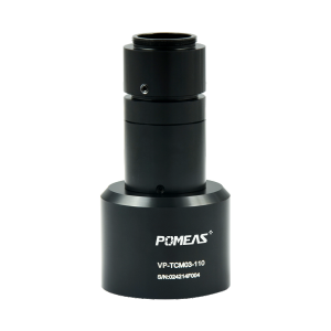
Product recommendation
TECHNICAL SOLUTION
MORE+You may also be interested in the following information
FREE CONSULTING SERVICE
Let’s help you to find the right solution for your project!

 ASK POMEAS
  PRICE INQUIRY
  REQUEST DEMO/TEST
  FREE TRIAL UNIT
  ACCURATE SELECTION
 - APPICATION CASE
- RESOURCE CENTER
- DOWNLOAD CENTER
SOLUTIONS SUPPORT
- ZOOM LENS SELECTION TOOL
- TELECENTRIC LENS SELECTION TOOL
- FA LENS SELECTION TOOL
- ZOOM RATIO TABLE
- CERTIFIED MODEL
SELECTION TOOL
- WHY POMEAS
- FAQ
- PRIVACY POLICY
- TERMS OF USE
- DELIVERY & RETURN POLICY
CUSTOMER CARE
 ADDRESS
Add.:No.68, Chongwei Road, Baizhoubian, East district, Dongguan, China, 523000
CONTACT
 Tel:+ 86-0769-2266 0867
 Fax:+ 86-0769-2266 0867
 E-mail:marketing@pomeas.com

Wechat QR code
Software Copyright :2021SR0176001 抄袭必究, 技术支持:誉新源科技