


In the fields of electronics manufacturing and semiconductor packaging, solder balls serve as critical interconnect materials, with their dimensional accuracy directly impacting device electrical performance and reliability. As electronic products evolve toward miniaturization and higher density, solder ball diameters have generally shrunk to 0.6mm or even smaller. However, measuring the dimensions of such ultra-micro components has long faced two major challenges: First, traditional measurement tools (such as calipers and projectors) struggle to achieve efficient inspection due to insufficient resolution or complex operation. Second, manual individual measurement is inefficient and prone to causing deformation of solder balls through contact-based handling, further compromising measurement accuracy.


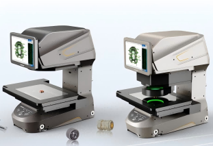
Against this backdrop, the POMEAS image measuring instrument has emerged as an innovative solution to the challenge of measuring 0.6mm solder balls, leveraging its non-contact, batch measurement capabilities and sub-micron precision.

I. Limitations of Traditional Measurement Methods
-
Insufficient Accuracy: Conventional measuring equipment (such as micrometers and optical projectors) typically has a resolution of 0.01mm, making it difficult to meet the tolerance requirement of ±0.005mm for 0.6mm solder balls. Additionally, contact-based measurement may cause deformation of solder balls due to uneven force application, introducing systematic errors.
-
Inefficient Process: Manual individual measurement requires repeated repositioning and focusing, taking approximately 30 seconds per solder ball. Inspecting thousands of solder balls consumes hours, while fatigue-induced human error becomes a significant risk.
-
Challenging Data Management: Traditional methods rely on manual data recording, hindering batch statistical analysis and trend tracking. This approach fails to meet modern production demands for quality traceability and process control.
II. Technical Breakthroughs in the POMEAS Image Measuring Instrument

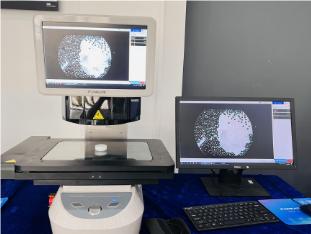
The POMEAS Image Measuring Instrument integrates high-resolution industrial lenses, intelligent algorithms, and automated control technology to achieve non-contact, batch-processing, high-precision measurement of 0.6mm solder balls. Its core advantages are as follows:
-
Sub-micron precision (0.001mm): Utilizing a combination of industrial cameras exceeding 20 million pixels and telecentric lenses, paired with sub-pixel edge extraction algorithms, enables precise identification of solder ball contours. Even when encountering reflective surfaces or slightly deformed solder balls, measurement repeatability remains ≤0.002mm.
-
100x Faster Batch Measurement Efficiency: Utilizing a multi-station stage and auto-focus functionality, it simultaneously measures 100-1000 solder balls per run without manual intervention. Batch measurement time is reduced to under 30 seconds, achieving over 100 times the efficiency of traditional methods.
-
Intelligent Data Analysis and Report Generation: The built-in Statistical Process Control (SPC) module calculates key metrics like CPK values and standard deviation in real time. It automatically generates ISO-compliant inspection reports and supports seamless integration with MES systems, enabling closed-loop quality data management.
III. Test Results

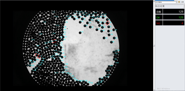
Achieve measurement of over 100 items at once

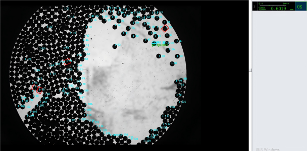
Measurement accuracy can reach 0.0001 mm
Product recommendation
TECHNICAL SOLUTION
MORE+You may also be interested in the following information
FREE CONSULTING SERVICE
Let’s help you to find the right solution for your project!

 ASK POMEAS
  PRICE INQUIRY
  REQUEST DEMO/TEST
  FREE TRIAL UNIT
  ACCURATE SELECTION
 - APPICATION CASE
- RESOURCE CENTER
- DOWNLOAD CENTER
SOLUTIONS SUPPORT
- ZOOM LENS SELECTION TOOL
- TELECENTRIC LENS SELECTION TOOL
- FA LENS SELECTION TOOL
- ZOOM RATIO TABLE
- CERTIFIED MODEL
SELECTION TOOL
- WHY POMEAS
- FAQ
- PRIVACY POLICY
- TERMS OF USE
- DELIVERY & RETURN POLICY
CUSTOMER CARE
 ADDRESS
Add.:No.68, Chongwei Road, Baizhoubian, East district, Dongguan, China, 523000
CONTACT
 Tel:+ 86-0769-2266 0867
 Fax:+ 86-0769-2266 0867
 E-mail:marketing@pomeas.com

Wechat QR code
Software Copyright :2021SR0176001 抄袭必究, 技术支持:誉新源科技