


What are the advantages of using a laser autofocus microscope system for wafer inspection?
In the semiconductor manufacturing sector, wafers serve as the core carriers for chip production, with their surface quality directly impacting the performance and yield of the final products. Traditional inspection methods, constrained by manual operation and mechanical contact, struggle to meet the micron-level or even nanometer-level precision demands of modern processes. Laser autofocus microscopy systems, leveraging their core advantages of automation, high precision, and non-contact operation, have emerged as a key technological breakthrough in wafer inspection. The following analysis explores their technical principles, core advantages, and practical application scenarios.

I. Technical Principle: Deep Integration of Laser Ranging and Microscopic Imaging

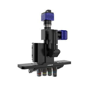
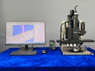
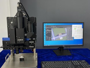
The laser autofocus microscope system integrates a laser sensor, industrial camera, coaxial light source, and precision motion modules to form a closed-loop “distance measurement-focusing-imaging” system. Its operating principle can be divided into three steps:
1. Laser Distance Measurement: The system emits a laser beam onto the wafer surface and calculates surface height information in real time by measuring the time-of-flight or phase difference of the reflected signal. For example, the POMEAS Focus system can capture micrometer-level height variations with an accuracy of ±0.1μm.
2. Autofocus: Based on distance measurement data, the system drives the objective lens movement module to adjust the focal length, ensuring the image remains in optimal focus at all times. This process requires no manual intervention, with a response time under 10 milliseconds—significantly faster than traditional mechanical focusing.
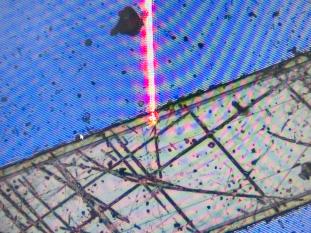
3. Microscopic imaging: APO objectives synergize with coaxial illumination to deliver high-resolution images. Industrial cameras capture wafer surface details at dozens of frames per second, enabling real-time defect analysis.
II. Core Advantages: Comprehensive Upgrades in Efficiency, Precision, and Reliability

1. High degree of automation reduces human error
Traditional inspection relies on manual focusing and observation by operators, making it susceptible to factors such as skill level and fatigue. Laser autofocus systems, driven by algorithms, achieve full-process automation:
- Autofocus: During wafer transport or inspection, the system continuously tracks surface height variations and dynamically adjusts focus to prevent image blur caused by vibration or displacement.
- Data Standardization: Inspection results are output as images or videos. Combined with AI analysis software, defects such as scratches, stains, and cracks can be automatically identified, reducing subjective judgment errors.
2. Fast detection speed meets the demands of large-scale production.
Wafer manufacturing demands extremely high inspection efficiency, requiring hundreds of points to be inspected on a single wafer within minutes. The laser autofocus system achieves high-speed inspection through the following design:
- Parallel Processing: The system can simultaneously perform distance measurement and imaging at multiple detection points. Combined with a multi-axis motion platform, it enables “detection while moving.”
- Rapid Response: The synergistic optimization of laser sensors and motion modules reduces focusing time to one-fifth of traditional methods, cutting single-wafer inspection time from 30 minutes to 6 minutes.
3. High-precision focusing, pushing the limits of micro- and nano-level detection
As chip line widths advance below 3nm, wafer surface defect sizes have reached the nanometer scale. Laser autofocus systems achieve high precision through the following technologies:
- Sub-micron Level Distance Measurement: Utilizing confocal laser principles combined with high-precision sensors, it can resolve height differences as small as 0.01μm, meeting the demands of advanced manufacturing processes.
- Anti-Interference Design: The system employs algorithms to filter out environmental disturbances such as vibrations and light fluctuations, ensuring stable distance measurement. For instance, in cleanroom environments, the system achieves repeatable positioning accuracy of ±0.05μm.
4. Non-contact inspection ensures wafer integrity
Traditional mechanical contact-based inspection methods risk scratching wafer surfaces and introducing contamination. The laser autofocus system employs a non-contact design, enabling non-destructive inspection through beam scanning:
- No physical contact: The laser beam does not directly contact the wafer surface, preventing microcracks or contamination caused by mechanical stress.
- Compatible with fragile materials: Safely inspects delicate materials such as ultra-thin wafers (thickness <50μm) and flexible substrates.
III. Practical Application Scenarios: Covering the Entire Wafer Manufacturing Process

1. Film Inspection: Monitors the uniformity and thickness of photoresist coating to ensure anti-oxidation layer performance.
2. Development and Etching Monitoring: Tracks etch depth and width in real time to prevent over-etching or under-etching.
3. Impurity Distribution Detection: Identifies concentration deviations in doped regions to optimize P/N-type semiconductor formation.
4. Chip Packaging Inspection: Measures bump height and coplanarity to guarantee signal transmission reliability.
Product recommendation
TECHNICAL SOLUTION
MORE+You may also be interested in the following information
FREE CONSULTING SERVICE
Let’s help you to find the right solution for your project!

 ASK POMEAS
  PRICE INQUIRY
  REQUEST DEMO/TEST
  FREE TRIAL UNIT
  ACCURATE SELECTION
 - APPICATION CASE
- RESOURCE CENTER
- DOWNLOAD CENTER
SOLUTIONS SUPPORT
- ZOOM LENS SELECTION TOOL
- TELECENTRIC LENS SELECTION TOOL
- FA LENS SELECTION TOOL
- ZOOM RATIO TABLE
- CERTIFIED MODEL
SELECTION TOOL
- WHY POMEAS
- FAQ
- PRIVACY POLICY
- TERMS OF USE
- DELIVERY & RETURN POLICY
CUSTOMER CARE
 ADDRESS
Add.:No.68, Chongwei Road, Baizhoubian, East district, Dongguan, China, 523000
CONTACT
 Tel:+ 86-0769-2266 0867
 Fax:+ 86-0769-2266 0867
 E-mail:marketing@pomeas.com

Wechat QR code
Software Copyright :2021SR0176001 抄袭必究, 技术支持:誉新源科技