


1. Highly automated, reducing reliance on manual labor

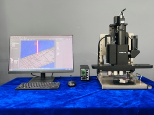
01. Intelligent Focus Control: Utilizing laser ranging and closed-loop feedback mechanisms, the system dynamically adjusts the distance between the objective lens and the wafer surface in real time, achieving stable focusing without manual intervention.
02. Typical Comparison: Traditional microscopes require operators to repeatedly adjust the Z-axis knob, a time-consuming process prone to errors due to fatigue. In contrast, the laser system performs the entire process autonomously, making it particularly suitable for batch inspection scenarios.
03. Extended Value: Supports integration with MES/ERP systems to enable fully automated inspection across production lines, significantly reducing labor costs.
2. Ultra-high-speed inspection, breaking through production capacity bottlenecks

01. Millisecond Response Speed: Laser-triggered autofocus locks onto the target plane within milliseconds. Combined with high-speed stage movement, single-wafer inspection time is reduced to one-third to one-fifth of traditional equipment.
02. Continuous Operation Capability: An automated process with no mechanical pauses, ideal for high-throughput wafer production demands.
03. Time Savings: For a single 12-inch wafer, conventional inspection takes 5 minutes, while this system completes it within 90 seconds, directly boosting overall equipment effectiveness.
3. Sub-micron AF Precision Ensures Detection Reliability

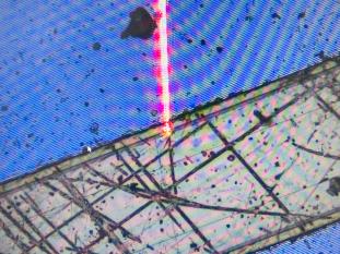
01. Nanometer-level repeatability: Piezoelectric ceramic motors (PZT) calibrated with helium-neon laser interferometers achieve vertical positioning accuracy of ±5nm, far surpassing the micrometer-level errors of manual adjustments.
02. Core technology support: Confocal principle + AI image recognition algorithms precisely distinguish true topography from out-of-focus artifacts, preventing over-detection or missed defects.
03. Quantified Outcomes: Detection rates for sub-14nm advanced process features—such as photoresist residues and particulate contamination—exceed traditional brightfield illumination by over 30%.
4. Enhanced Full-Process Quality Control
01. Eliminate Subjective Judgment Variations: Standardized optical parameters (wavelength/numerical aperture/illumination intensity) eliminate judgment errors caused by operator experience.
02. Big Data Traceability System: Each image frame includes metadata such as focal length compensation values and coordinate positions, facilitating defect traceability and process review.
03. Enhanced foolproof mechanism: The system automatically pauses and triggers an alarm upon detecting abnormally tilted wafers, preventing collision accidents and safeguarding expensive samples.
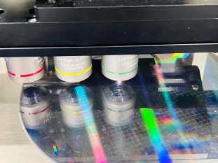
5. Multi-dimensional Application Scalability
01. Cross-Process Adaptability: From measuring film thickness on polished flat surfaces to inspecting steep aspect ratio trenches after etching, the system automatically adjusts depth-of-field range through algorithmic adaptation.
02. Special Material Compatibility: For samples with highly variable reflectivity, such as semiconductors and transparent substrates, optional multi-wavelength light source modules are available.
03. Intelligent Iteration Potential: The accumulated inspection database can be used to train deep learning models, continuously optimizing threshold segmentation and classification accuracy.
Product recommendation
TECHNICAL SOLUTION
MORE+You may also be interested in the following information
FREE CONSULTING SERVICE
Let’s help you to find the right solution for your project!

 ASK POMEAS
  PRICE INQUIRY
  REQUEST DEMO/TEST
  FREE TRIAL UNIT
  ACCURATE SELECTION
 - APPICATION CASE
- RESOURCE CENTER
- DOWNLOAD CENTER
SOLUTIONS SUPPORT
- ZOOM LENS SELECTION TOOL
- TELECENTRIC LENS SELECTION TOOL
- FA LENS SELECTION TOOL
- ZOOM RATIO TABLE
- CERTIFIED MODEL
SELECTION TOOL
- WHY POMEAS
- FAQ
- PRIVACY POLICY
- TERMS OF USE
- DELIVERY & RETURN POLICY
CUSTOMER CARE
 ADDRESS
Add.:No.68, Chongwei Road, Baizhoubian, East district, Dongguan, China, 523000
CONTACT
 Tel:+ 86-0769-2266 0867
 Fax:+ 86-0769-2266 0867
 E-mail:marketing@pomeas.com

Wechat QR code
Software Copyright :2021SR0176001 抄袭必究, 技术支持:誉新源科技