


Line Laser Profile Scanning Sensor—High-Precision Measurement for Electronics
Measurement Background: Why Focus on the Height of Small Components on Electronic Devices?

1、Ensuring product quality and reliability
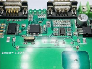
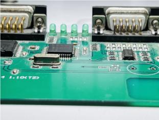
In modern electronics manufacturing, circuit boards are densely populated with various miniature components such as chips, resistors, and capacitors. The height of these components directly impacts the overall assembly quality and electrical performance of the circuit board. If heights exceed design specifications, issues like short circuits between adjacent pins or poor solder joints may occur, potentially leading to equipment malfunctions or even safety hazards. Precise measurement of small component heights enables timely detection of deviations during production, ensuring each component meets design specifications. This safeguards the long-term stable operation of electronic products.

2、Adapt to the demands of precision manufacturing
As electronic products continue to evolve toward thinner, lighter, and higher-performance designs, demands for component dimensions and spacing grow increasingly stringent. Traditional measurement methods struggle to meet the high-precision, high-efficiency requirements of production, particularly in mass manufacturing scenarios where rapidly and accurately capturing height data for large volumes of components becomes critical. Consequently, identifying a detection method capable of micrometer-level precision and high-speed measurement represents an urgent challenge for the electronics manufacturing industry.
Measurement Solution: Line Laser Profile Scanning Sensor

1、Overview of Technical Principles

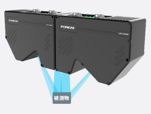
The line laser profile scanning sensor operates based on the principle of optical triangulation. It emits a narrow band of laser light onto the surface of the object being measured. Due to variations in the surface topography, the reflected light becomes scattered. An internal image sensor captures this scattered light. By analyzing the laser's incident angle, the position of the reflected light, and pre-calibrated geometric relationships, the sensor calculates height data for each point on the object's surface. This non-contact measurement method causes no damage to the object being measured, making it particularly suitable for fragile or easily deformed electronic components.
2、System Composition and Deployment

- A high-resolution, high-precision line laser profile scanning sensor is selected as the primary measurement tool. This sensor must feature a small spot size and high sampling frequency to meet the precise measurement requirements for minute components.
- To cover the entire circuit board area, it is typically paired with a two-dimensional or three-dimensional precision motion platform. The motion platform guides the circuit board along a preset path, enabling the laser to sequentially scan each component under test. The motion platform must achieve high repeatability to ensure consistency across multiple measurements.
- A robust computer control system is integrated to collect sensor data and perform real-time processing and analysis. Software algorithms filter and fit the raw data to extract precise component height values, then visualize the results for operators to intuitively understand measurement outcomes.

3、Detailed Explanation of the Measurement Process
1. Calibration Phase: Prior to use, perform comprehensive calibration of the line laser profile scanning sensor. This includes zero calibration—establishing the reference plane when no object is present—and range calibration—verifying the sensor's linearity and accuracy across varying height ranges. This step ensures the reliability of subsequent measurement results.
2. Mounting and Securing: Place the electronic board to be tested steadily on the motion platform. Secure it firmly using specialized fixtures to prevent displacement during measurement. For larger boards, segmented measurements may be performed, with markings applied at the joints for subsequent data integration.
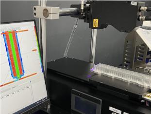
3. Scanning Measurement: Activate the motion platform to move slowly along the preset speed and trajectory while the line laser profile sensor continuously emits laser beams and collects data. During this process, the sensor records height information from the surface of each component on the PCB, generating detailed 3D point cloud data.
4. Data Analysis and Report Generation: The computer control system processes the received data, identifies the position and boundaries of each component, calculates their height values, and compares them against preset standard thresholds. If any deviation beyond the tolerance range is detected, the system automatically triggers an alarm. Finally, a report is generated containing measurement results, statistical analysis charts, and pass/fail conclusions for archiving and traceability by the quality department.
Distinct Advantages: The Unique Value of Line Laser Profile Scanning Sensors
1. Rapid and Efficient, Significantly Boosting Production Capacity
Line laser profile scanning sensors capture two-dimensional contour information from multiple points along an entire line in a single scan. Compared to traditional point-by-point measurement methods, this dramatically increases measurement speed. Particularly when handling high-volume production of electronic boards, it can complete height measurements for a large number of components in a short time, effectively shortening production cycles and enhancing corporate production efficiency.
2. Non-contact measurement protects sensitive components
Utilizing optical measurement principles, it requires no direct contact with the object being measured, preventing damage or deformation caused by mechanical pressure. This is particularly crucial for electronic components with thin surface coatings or fragile materials, ensuring both safety and accuracy during the measurement process.
3. Batch measurement meets full inspection requirements
In electronics manufacturing, full inspection rather than sampling is often required to guarantee product quality. The line laser profile scanning sensor effortlessly measures all components on an entire circuit board simultaneously. It rapidly and accurately captures height data for both regularly arranged and irregularly distributed components, fulfilling the full inspection demands of large-scale production.
4. High Flexibility for Diverse Applications
This sensor offers flexible configuration based on PCB dimensions, component layouts, and measurement requirements. By adjusting laser parameters, motion platform speed/trajectory, and data processing algorithms, it adapts to complex measurement tasks. Effective measurements are achieved for single-sided or multi-layer boards, standard or irregularly shaped components.
5. Rich Data for In-Depth Analysis
Beyond providing basic height values, the line laser profile scanner generates detailed 3D point cloud data and 2D cross-sectional images. This comprehensive data not only verifies component height compliance but also enables further analysis of geometric properties like flatness and tilt. This provides valuable insights for production process optimization and troubleshooting quality issues.
Product recommendation
TECHNICAL SOLUTION
MORE+You may also be interested in the following information
FREE CONSULTING SERVICE
Let’s help you to find the right solution for your project!

 ASK POMEAS
  PRICE INQUIRY
  REQUEST DEMO/TEST
  FREE TRIAL UNIT
  ACCURATE SELECTION
 - APPICATION CASE
- RESOURCE CENTER
- DOWNLOAD CENTER
SOLUTIONS SUPPORT
- ZOOM LENS SELECTION TOOL
- TELECENTRIC LENS SELECTION TOOL
- FA LENS SELECTION TOOL
- ZOOM RATIO TABLE
- CERTIFIED MODEL
SELECTION TOOL
- WHY POMEAS
- FAQ
- PRIVACY POLICY
- TERMS OF USE
- DELIVERY & RETURN POLICY
CUSTOMER CARE
 ADDRESS
Add.:No.68, Chongwei Road, Baizhoubian, East district, Dongguan, China, 523000
CONTACT
 Tel:+ 86-0769-2266 0867
 Fax:+ 86-0769-2266 0867
 E-mail:marketing@pomeas.com

Wechat QR code
Software Copyright :2021SR0176001 抄袭必究, 技术支持:誉新源科技