


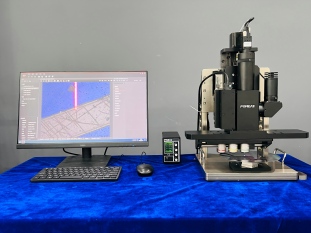
In high-precision industrial fields such as semiconductor manufacturing, precision machining, and LCD screen inspection, the performance of inspection equipment directly determines product quality and production efficiency. Leveraging its technological advantages, the POMEAS Focus X Laser Auto-Focus Microscope System has become the core tool for industry users to enhance their inspection capabilities.

I. Micron-Level Precision and 6.5kHz High-Speed Focusing: Pushing Beyond Traditional Detection Limits

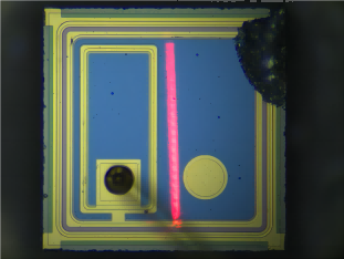
The Focus X system employs coaxial laser focusing technology, utilizing a semiconductor laser to emit a precise beam. Combined with a high-speed signal processing module, it achieves micrometer-level focusing accuracy and a dynamic response speed of 6.5 kHz. In semiconductor wafer inspection, this system can detect uniformity variations in coating thickness as small as 0.1 micrometers, delivering a 300% efficiency improvement over traditional contact probe inspection methods.
II. Non-contact Detection: A Revolutionary Design for Preserving Sample Integrity

Traditional microscopic inspection relies on mechanical probes contacting the sample surface, which can easily cause scratches, electrostatic damage, or contamination. The Focus X system employs laser confocal imaging technology to non-invasively scan the surface topography of samples. In LCD screen inspection scenarios, this system enables non-destructive testing of flexible OLED screens, avoiding pixel damage caused by contact pressure from traditional piezoelectric sensors.
III. Dynamic Surface Adaptability: Covering the Full Range of Testing Needs Across the Entire Industry Chain

The system's built-in laser sensor module supports both static and dynamic dual-focus modes, enabling real-time tracking of moving sample surfaces. In precision laser welding applications, the system locks onto the dynamic deformation of the weld pool at a 10kHz update rate, ensuring real-time monitoring of weld seam quality.
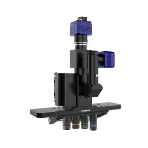
IV. Modular Integrated Design: Lowering the Barrier to Industrial System Retrofits

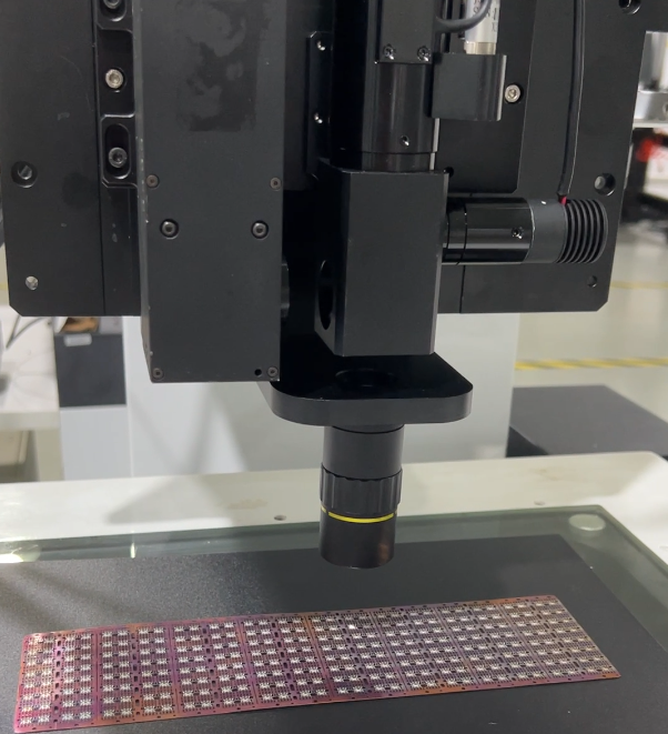
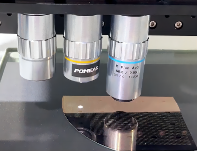
The Focus X features a compact, integrated design that houses core modules—including laser control, motion control, and software algorithms—within a cylindrical chamber measuring 150mm in diameter. Its compatibility with 2x-100x universal objectives enables seamless integration with existing microscope systems.
V. Multi-Industry Scenario Coverage: Comprehensive Applications from Micro to Macro Dimensions

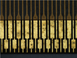
1. Semiconductor Manufacturing: During wafer development and etching processes, the system enables real-time monitoring of pattern transfer accuracy at 0.5μm line widths, ensuring the integrity of chip circuit layouts.
2. 3C Electronics Inspection: For smartphone case screw hole inspection, the system rapidly locates screw holes at varying heights using a zoom objective, reducing inspection cycle time to 8 seconds per unit.
3. New Energy Sector: In photovoltaic silicon wafer cutting quality inspection, the system identifies 0.3μm-level chipping defects, boosting N-type cell conversion efficiency by 0.5%.
4. Biomedical Applications: Enables real-time 3D morphology reconstruction of cell culture dishes, providing micrometer-level morphological data for tissue engineering.
Product recommendation
TECHNICAL SOLUTION
MORE+You may also be interested in the following information
FREE CONSULTING SERVICE
Let’s help you to find the right solution for your project!

 ASK POMEAS
  PRICE INQUIRY
  REQUEST DEMO/TEST
  FREE TRIAL UNIT
  ACCURATE SELECTION
 - APPICATION CASE
- RESOURCE CENTER
- DOWNLOAD CENTER
SOLUTIONS SUPPORT
- ZOOM LENS SELECTION TOOL
- TELECENTRIC LENS SELECTION TOOL
- FA LENS SELECTION TOOL
- ZOOM RATIO TABLE
- CERTIFIED MODEL
SELECTION TOOL
- WHY POMEAS
- FAQ
- PRIVACY POLICY
- TERMS OF USE
- DELIVERY & RETURN POLICY
CUSTOMER CARE
 ADDRESS
Add.:No.68, Chongwei Road, Baizhoubian, East district, Dongguan, China, 523000
CONTACT
 Tel:+ 86-0769-2266 0867
 Fax:+ 86-0769-2266 0867
 E-mail:marketing@pomeas.com

Wechat QR code
Software Copyright :2021SR0176001 抄袭必究, 技术支持:誉新源科技