What is a telecentric lens?


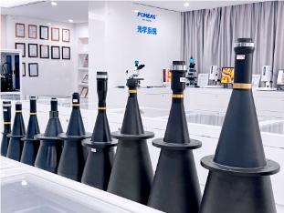
Telecentric lenses are a specialized type of optical lens designed to eliminate parallax errors. They ensure that the magnification of points on an object remains constant within a specific object distance range, preventing measurement errors caused by shifts in the object's position within the object plane or its movement forward or backward. Compared to standard optical lenses, telecentric lenses prioritize imaging accuracy and stability, making them particularly suitable for high-precision measurement and inspection applications.
Telephoto Lens Classification and Applications
1. Parallax-free lens: Its primary feature is that the principal rays of incident light are parallel to the lens's optical axis, effectively eliminating measurement errors caused by object movement along the optical axis. It is suitable for measuring dimensions such as PCB thickness and component height.
2. Image-side telecentric lens: The principal rays of the imaging light are parallel to the optical axis, reducing the impact of detector (e.g., camera sensor) positional shifts on imaging accuracy. Commonly used for clear imaging inspection of minute defects on PCBs (e.g., circuit scratches, pad notches).
3. Bilateral telecentric lens: Combines both object-side and image-side telecentric properties, eliminating errors from object movement while also mitigating effects of detector position shifts. This makes it an ideal choice for high-precision PCB inspection, such as measuring fine circuit dimensions or verifying component pin spacing.
Core Requirements for PCB Inspection and Compatibility with Telephoto Lenses
PCBs (printed circuit boards), as the core carriers of electronic devices, directly impact the performance and reliability of such equipment. PCB inspection primarily covers three key requirements: dimensional accuracy inspection, defect detection, and component assembly verification. The characteristics of telecentric lenses align exceptionally well with these demands:
- Dimensional Accuracy Requirements: PCB boards demand extremely high precision for line widths, spacing, pad diameters, and component pin pitches (often reaching micrometer levels). Conventional lenses suffer from parallax errors, making measurement results susceptible to object positioning. The constant magnification characteristic of telecentric lenses ensures dimensional measurement errors below 0.1%.
- Defect Detection Requirements: Common PCB defects like short circuits/open circuits, pad oxidation, solder joint defects, and foreign object residues are small and low-contrast. Telecentric lenses' high resolution and low distortion clearly reveal defect details, preventing missed or false detections caused by imaging distortion.
- Assembly Consistency Requirements: PCB component assembly must guarantee consistent component positioning and height. Telecentric lenses precisely capture three-dimensional positional data, aiding in the detection of component misalignment, tilt, or missing parts.
Specific Application Scenarios of Telecentric Lenses in PCB Inspection


(1) PCB Board Dimension Measurement
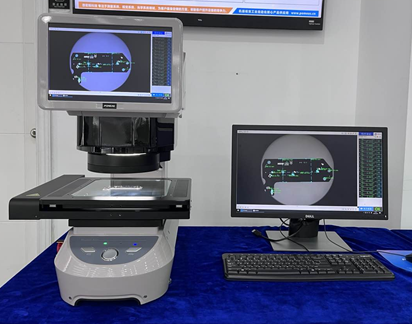
- Line Width and Spacing Measurement: Following the etching process in PCB manufacturing, it is necessary to verify whether the line width and spacing meet design specifications (e.g., 0.1mm line width with ±0.01mm tolerance). Using a dual-side telecentric lens paired with a high-resolution industrial camera captures clear images of PCB traces. Combined with machine vision algorithms (such as edge detection), this system precisely extracts trace edge coordinates to calculate line width and spacing with measurement accuracy reaching ±2μm.
- Pad Size and Position Inspection: Pad diameter and center position directly impact subsequent component soldering quality. The telecentric lens eliminates measurement errors caused by surface height variations (e.g., variations in tin plating thickness). It determines the deviation between the actual pad dimensions and design coordinates through imaging, ensuring the deviation is controlled within 0.05mm.
- Board Thickness and Via Diameter Measurement: For multilayer PCBs, board thickness uniformity and via diameter must be inspected. A non-contact board thickness measurement is achieved using a rectilinear telecentric lens combined with a laser displacement sensor. For vias, dual telecentric lenses capture the hole's orthographic projection to calculate diameter and positional deviation, eliminating measurement errors caused by the “near-large-far-small” distortion inherent in standard lenses.
(2) PCB Defect Detection
- Circuit Defect Detection: Common defects include short circuits (abnormal connectivity between adjacent circuits), open circuits (circuit breaks), and scratches (surface damage to circuits). Telecentric lenses can clearly image circuit details, enabling identification of even minute scratches (e.g., 0.02mm wide, 0.1mm long) through gray-scale contrast differences. For short-circuit defects, the low distortion characteristic of telecentric lenses prevents overlapping circuit images, allowing accurate determination of the short-circuit area.
- Solder Pad Defect Detection: Oxidation (darkened surface), notches (edge defects), and foreign matter adhesion (e.g., solder residue) compromise solder joint conductivity. A telecentric lens paired with a ring light enhances contrast on the pad surface. Oxidized areas appear as dark zones due to reduced reflectivity, while notches manifest as incomplete edges. Foreign matter stands out through grayscale differences, achieving detection accuracy exceeding 99.5%.
- Through-hole defect detection: Blocked through-holes (due to metal debris or resin residue) and poor plating on hole walls (insufficient plating thickness or peeling) can cause signal transmission failures. Dual-side telecentric lenses capture vertical images of through-holes, where blockages appear as dark areas within the holes, while plating defects are identified through uneven grayscale on the hole walls. Combined with image analysis, this enables rapid screening of non-conforming through-holes.
(3) PCB Component Assembly Inspection
- Component Position Deviation Detection: Following SMT (Surface Mount Technology) assembly, components such as resistors, capacitors, and chips may exhibit positional deviations (e.g., X/Y-axis shifts or rotational misalignment). Telecentric lenses capture the component's orthographic projection image. By comparing the actual component position against the design coordinates, the deviation amount is calculated (e.g., deviations exceeding 0.1mm are deemed non-compliant). Simultaneously, the system detects whether components are missing.
- Component Height and Coplanarity Inspection: Certain components (such as BGA ball grids and connectors) require consistent height and pin coplanarity to prevent solder joint failure. Objective telecentric lenses combined with triangulation principles capture component height data to determine height deviations (e.g., BGA ball height deviation must be ≤0.03mm). For pin coplanarity, imaging detects height variations to ensure coplanarity meets specifications.
Advantages of Telephoto Lenses in PCB Inspection
- Low distortion rate: Telecentric lenses typically exhibit distortion rates below 0.1%, significantly lower than conventional industrial lenses (which often have distortion rates of 1%-5%). This minimizes detection errors caused by image distortion, making them particularly suitable for inspecting intricate PCB structures such as fine traces and pins.
- No measurement parallax: Conventional lenses produce parallax due to changes in object distance, resulting in inconsistent measurement results for different positions on the same object. Telecentric lenses employ a specialized optical design to eliminate parallax within a specified object distance range, ensuring consistent measurement accuracy at any position on the object.
- High Resolution and High Contrast: Telecentric lenses utilize high-transmittance optical glass and multi-layer coating technology to minimize light reflection and scattering. This enhances image resolution (up to 12 megapixels) and contrast, clearly revealing minute defects and intricate structures on PCBs.
- Adaptable to diverse inspection environments: Telecentric lenses can be paired with light sources of different wavelengths (such as visible light, ultraviolet light, and infrared light) to accommodate various PCB inspection scenarios (e.g., transparent substrate inspection and component marking recognition). Additionally, some telecentric lenses feature dustproof and fog-proof designs, enabling stable operation in dusty and humid PCB production environments.


Telecentric lenses, with their low distortion, zero parallax, and high resolution, have become the core optical components for high-precision PCB inspection. They play an irreplaceable role in scenarios such as dimensional measurement, defect detection, and component assembly inspection.
Product recommendation
TECHNICAL SOLUTION
MORE+You may also be interested in the following information
FREE CONSULTING SERVICE
Let’s help you to find the right solution for your project!


 ASK POMEAS
  PRICE INQUIRY
  REQUEST DEMO/TEST
  FREE TRIAL UNIT
  ACCURATE SELECTION
  ADDRESS
 Tel:+ 86-0769-2266 0867
 Fax:+ 86-0769-2266 0867
 E-mail:marketing@pomeas.com
