


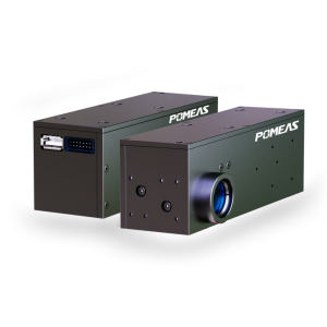
Advantages and Application Cases of Laser Image Auto-Focus Tracking Systems
In high-precision industrial fields such as semiconductor manufacturing, precision laser processing, and power battery production, traditional inspection technologies face multiple challenges: accuracy bottlenecks in micron-level defect detection, focusing delays in dynamic scenarios, imaging distortion on complex material surfaces, and efficiency losses from multi-device coordination. The POMEAS LFS Series Laser Image Auto-Focus Tracking System redefines industrial inspection standards by integrating linear laser technology, image processing, and intelligent tracking. It delivers micron-level precision, millisecond response times, and full-scenario adaptability as its core advantages.

I. Technical Advantages of the Laser Image Auto-Focus Tracking System
1. Multi-mode focusing delivers breakthroughs in both precision and speed.
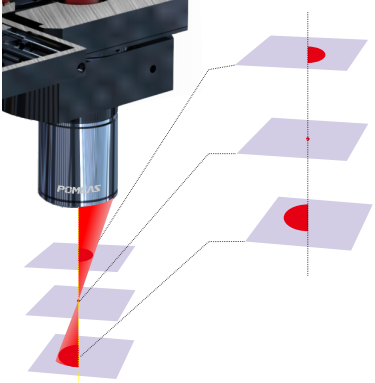
The LFS series' innovative hybrid autofocus mode intelligently switches between laser focusing and image focusing by analyzing target surface features in real time:
- Laser Focusing Mode: Utilizing a coaxial laser transmission and reception system, it calculates defocus distance by analyzing spot morphology, achieving a 6.5kHz-level focusing speed. Suitable for dynamic scenarios such as wafer dicing and power battery tab welding.
- Image Focusing Mode: Utilizing DSP-based high-speed image processing algorithms, this mode achieves sub-micron precision through contrast analysis and phase detection. It meets requirements for semiconductor wafer coating uniformity inspection and aerospace titanium alloy cutting verticality control. When cutting titanium alloy thin sheets, the system dynamically adjusts the cutting head position to maintain verticality error within 0.005mm.
- Hybrid Mode: Combining the speed advantage of laser technology with the precision advantage of imaging, this mode employs intelligent algorithms to eliminate interference from laser bad pixels. It maintains high-speed responsiveness while reducing focusing errors to one-third of those in traditional systems.
2. Full-scenario adaptation, solving complex material inspection challenges
The LFS series overcomes the limitations of traditional inspection technologies on material surfaces through optimized optical design and algorithmic modeling:
- High-contrast pattern surface: Leveraging the inverted characteristics of the laser spot, it precisely identifies minute height differences between circuit lines and the substrate on the wafer surface, preventing misjudgments caused by reflections or texture interference.
- High-magnification lens with minimal structure: Compatible with 2X-100X APO objectives, enabling clear imaging of micron-scale structures such as chip packaging bumps and micro-components. During 12-inch Mini LED wafer inspection, the system achieves rapid appearance inspection of millions of units through real-time continuous focusing and line-scan camera stitching.
- Multi-layer refractive index materials: For scenarios such as laminated glass and layered composites, the system employs multi-wavelength laser confocal measurement to penetrate surface reflection interference and directly acquire underlying structural data. In photovoltaic cell inspection, it can precisely identify interface defects between silicon layers and coating layers.
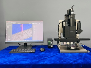
3. Closed-loop control, building a stable testing ecosystem
The LFS series incorporates a Z-axis closed-loop control system, integrating laser sensors, motion actuators, and software algorithms:
- Hardware Layer: Utilizes a piezoelectric ceramic-driven objective lens focusing module with a response time below 1 millisecond and repeatable positioning accuracy of ±0.1 micrometers.
- Software Layer: Features a web application-style interface supporting JavaScript frameworks, enabling customizable integration into existing AOI systems. Also provides RS-232 communication interfaces and multi-channel motor control functionality.
- Diagnostic Layer: Built-in sensor parameter monitoring and motor limit protection provide real-time feedback on focusing status, reducing equipment failure rates.
II. Industry Applications of Laser Image Auto-Focus Tracking Systems

1. Semiconductor Manufacturing
During wafer manufacturing, the LFS series can monitor coating thickness, etch depth, and impurity distribution in real time:
- Coating Inspection: Identifies uneven coating areas with micrometer-level precision to prevent wafer scrap caused by oxide layer defects.
- Development and Etching Monitoring: Dynamically adjust focus parameters to ensure etching width deviation remains below 0.5μm, thereby enhancing transistor integration density.
- Chip Packaging Inspection: Precisely measuring bump height and coplanarity reduces signal transmission failure rates to below 0.1%.
2. Precision Laser Processing
In the field of laser welding and cutting, the LFS series compensates for thermal deformation of workpieces and clamping errors:
- Power Battery Tab Welding: Real-time tracking of electrode stack displacement, controlling welding deviation within 2μm.
- Aerospace Titanium Alloy Cutting: Continuously monitor surface height variations to prevent structural strength degradation caused by beveled cuts.
3. Display Panel Manufacturing
For emerging display technologies such as flexible OLED and Mini LED, the LFS series resolves imaging distortion caused by insufficient depth of field:
- TFT Panel Polarizer Inspection: Utilizing a coaxial polarization system to achieve micron-level defect detection.
- 12-inch wafer disk visual inspection: By utilizing real-time continuous autofocus and image stitching, inspection efficiency is tripled.
Product recommendation
TECHNICAL SOLUTION
MORE+You may also be interested in the following information
FREE CONSULTING SERVICE
Let’s help you to find the right solution for your project!

 ASK POMEAS
  PRICE INQUIRY
  REQUEST DEMO/TEST
  FREE TRIAL UNIT
  ACCURATE SELECTION
 - APPICATION CASE
- RESOURCE CENTER
- DOWNLOAD CENTER
SOLUTIONS SUPPORT
- ZOOM LENS SELECTION TOOL
- TELECENTRIC LENS SELECTION TOOL
- FA LENS SELECTION TOOL
- ZOOM RATIO TABLE
- CERTIFIED MODEL
SELECTION TOOL
- WHY POMEAS
- FAQ
- PRIVACY POLICY
- TERMS OF USE
- DELIVERY & RETURN POLICY
CUSTOMER CARE
 ADDRESS
Add.:No.68, Chongwei Road, Baizhoubian, East district, Dongguan, China, 523000
CONTACT
 Tel:+ 86-0769-2266 0867
 Fax:+ 86-0769-2266 0867
 E-mail:marketing@pomeas.com

Wechat QR code
Software Copyright :2021SR0176001 抄袭必究, 技术支持:誉新源科技