


I. Technical Principles and Core Advantages

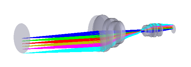
1. Eliminate perspective distortion: Utilizing a telecentric optical path on the object side and an aperture diaphragm on the image side ensures that principal rays remain strictly parallel to the optical axis. This maintains consistent image size for objects at varying distances, completely eliminating the “near large, far small” issue common in standard lenses. Typical measurement errors can be controlled within 0.1%.
2. Suppressing Reflections and Shadows: Utilizing an integrated ring light or an external coaxial light module, light strikes the object surface perpendicular to the optical axis. Reflected light returns along the original path to the lens, effectively reducing interference from reflections on transparent materials (e.g., glass, LCD panels) or mirror-like objects. In semiconductor wafer inspection, this enhances contrast for surface defects on chips by over 30%.
3. Low Distortion and High Resolution: Paired with high-resolution sensors (e.g., 2/3-inch 12-megapixel), it achieves 4μm/pixel resolution at an 80mm working distance, meeting micrometer-level measurement requirements.
II. Key Selection Criteria

-
Magnification and Working Distance: These must be matched to the dimensions of the target object and the sensor's active area. For example, when detecting a 10mm×10mm object with a 2/3-inch sensor (17mm×13mm), select a magnification of 0.6-1.0X. Working distance must account for installation space for lighting and mechanical structures.
-
Balance Between Depth of Field and Resolution: A larger depth of field enhances adaptability to surface undulations of objects. The typical depth of field range is 0.1–2.5 mm, suitable for flat objects with minimal height variations. Resolution is determined by numerical aperture (NA); a higher NA yields higher resolution.
-
Telecentricity and Distortion Control: Industrial standards require telecentricity ≤0.05°, ensuring edge field-of-view size error remains below 0.02%. Distortion can be further compensated through software algorithms like polynomial fitting. For instance, when inspecting precision gears, corrected measurement accuracy can be enhanced to ±1μm.
-
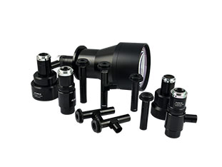
Light Source and Interface Compatibility: Select illumination wavelength based on material properties. For instance, green light (525nm) enhances defect contrast on metal surfaces. Interfaces primarily use C-mount, requiring compatibility with camera sensor size (e.g., 2/3-inch) and interface protocols (e.g., USB3.0, GigE).
III. Typical Application Scenarios

-
Semiconductor and Electronics Manufacturing: Utilizing POMEAS standard telecentric series lenses with coaxial illumination enables detection of 0.5μm-level scratches and particle defects on wafers. At a 65mm working distance, it achieves measurement accuracy of ±2μm for PCB pad spacing.
-
Automotive Parts Inspection:Telecentric lenses combined with AI algorithms enable rapid detection of precision gear tooth profile errors, boosting pass rates to 99.8%. The standard telecentric depth-of-field design accommodates measurement of minute deformations after connector terminal insertion and removal.
-
Optical Components and Materials Science:Using coaxial optical interference combined with high-precision focusing via telecentric lenses enables glass wafer thickness measurement with ±0.5μm accuracy. In the packaging industry, coaxial illumination significantly enhances detection sensitivity for wrinkles as small as 0.1mm on transparent film surfaces.
Product recommendation
TECHNICAL SOLUTION
MORE+You may also be interested in the following information
FREE CONSULTING SERVICE
Let’s help you to find the right solution for your project!

 ASK POMEAS
  PRICE INQUIRY
  REQUEST DEMO/TEST
  FREE TRIAL UNIT
  ACCURATE SELECTION
 - APPICATION CASE
- RESOURCE CENTER
- DOWNLOAD CENTER
SOLUTIONS SUPPORT
- ZOOM LENS SELECTION TOOL
- TELECENTRIC LENS SELECTION TOOL
- FA LENS SELECTION TOOL
- ZOOM RATIO TABLE
- CERTIFIED MODEL
SELECTION TOOL
- WHY POMEAS
- FAQ
- PRIVACY POLICY
- TERMS OF USE
- DELIVERY & RETURN POLICY
CUSTOMER CARE
 ADDRESS
Add.:No.68, Chongwei Road, Baizhoubian, East district, Dongguan, China, 523000
CONTACT
 Tel:+ 86-0769-2266 0867
 Fax:+ 86-0769-2266 0867
 E-mail:marketing@pomeas.com

Wechat QR code
Software Copyright :2021SR0176001 抄袭必究, 技术支持:誉新源科技