


Deep-Focus Telephoto Lenses for Measurement Applications in the Electronics Industry
Core Competitive Advantages

01. Constant magnification and no perspective error:
Telecentric lenses employ a parallel optical path design, ensuring that object size measurements within the depth of field remain unaffected by changes in object distance. This eliminates perspective errors where objects appear larger up close and smaller in the distance, making them ideal for precision inspection of electronic components—such as IC chips, resistors, and capacitors—for dimensional accuracy, positioning, and solder joint quality. In PCB board inspection, they enable precise measurement of trace width, solder joint spacing, and surface defects (e.g., cold solder joints, short circuits), ensuring compliance with design specifications.
02. Low distortion and high resolution:
Telecentric lenses exhibit extremely low distortion rates (typically <0.1%), delivering sharp edge imaging ideal for inspecting minute structures (e.g., chip line widths, screen pixel defects) and surface micro-defects (e.g., scratches, pits, corrosion). Combined with high-resolution imaging, they achieve micron-level or even nanometer-level precision, meeting demanding requirements in scenarios such as semiconductor wafer defect detection and chip packaging dimensional verification.
03. Deep depth of field and wide working range:
The large depth of field capability enables clear imaging of objects at different heights within the same working distance, reducing refocusing frequency and enhancing inspection efficiency. For instance, when inspecting deformable objects such as rubber seals or plastic caps, non-contact measurement can be performed without physical contact, eliminating errors caused by physical interaction. Suitable for three-dimensional structural inspection (e.g., surface undulations on electronic components or complex curved surfaces), it can achieve 3D contour reconstruction and dimensional analysis when integrated with a stereo vision system.
04. Automation Integration Capabilities:
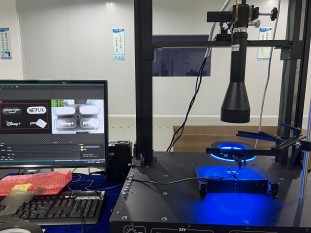
When integrated with machine vision systems (such as industrial cameras and image processing software), it enables automated online inspection, providing real-time feedback on product quality information. This reduces manual intervention and enhances production line efficiency. For example, on automated assembly lines, telecentric lenses can rapidly identify component positions, inspect solder joint quality, and automatically reject non-conforming products.
Specific application scenarios

01. Semiconductor and Electronics Manufacturing: Wafer defect detection, chip package dimension measurement, microstructure analysis (e.g., TSV through-holes, BGA solder joints). Precision circuit board inspection (e.g., HDI boards, flexible PCBs) for trace width, hole position accuracy, and surface defect detection.
02. Surface Quality Inspection: Detection of dark areas and color variations on smartphone screen bezels; identification of scratches and pits on metal surfaces; analysis of surface defects on plastic components.
03. Automated Production Lines: Real-time online inspection of electronic component dimensions, positioning, and cosmetic defects. Integration with robotic vision guidance enables precise assembly, sorting, and packaging integrity verification (e.g., food/pharmaceutical packaging boxes, bottle inspection).
04. 3D Measurement and Complex Structure Analysis: Utilizes laser scanning or structured light technology for 3D contour measurement and surface topography analysis. Suitable for dimensional verification of precision mechanical parts and automotive electronic components.
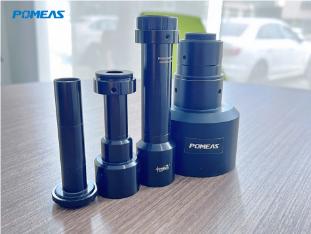
Product recommendation
TECHNICAL SOLUTION
MORE+You may also be interested in the following information
FREE CONSULTING SERVICE
Let’s help you to find the right solution for your project!

 ASK POMEAS
  PRICE INQUIRY
  REQUEST DEMO/TEST
  FREE TRIAL UNIT
  ACCURATE SELECTION
 - APPICATION CASE
- RESOURCE CENTER
- DOWNLOAD CENTER
SOLUTIONS SUPPORT
- ZOOM LENS SELECTION TOOL
- TELECENTRIC LENS SELECTION TOOL
- FA LENS SELECTION TOOL
- ZOOM RATIO TABLE
- CERTIFIED MODEL
SELECTION TOOL
- WHY POMEAS
- FAQ
- PRIVACY POLICY
- TERMS OF USE
- DELIVERY & RETURN POLICY
CUSTOMER CARE
 ADDRESS
Add.:No.68, Chongwei Road, Baizhoubian, East district, Dongguan, China, 523000
CONTACT
 Tel:+ 86-0769-2266 0867
 Fax:+ 86-0769-2266 0867
 E-mail:marketing@pomeas.com

Wechat QR code
Software Copyright :2021SR0176001 抄袭必究, 技术支持:誉新源科技