


Understand the Hardware Components and Functions of a White Light Interferometer in 1 Minute
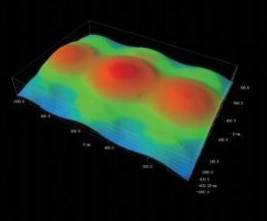
White light interferometry 3D profilometers serve as powerful tools for nanometer-level precision measurement, with their core functionality based on the principle of white light interference. The illumination beam is split into two beams by a half-silvered mirror: one beam is projected onto the sample surface, while the other is directed onto the reference mirror surface. The two reflected beams converge again, forming interference fringes on the CCD camera's photosensitive surface. By analyzing the brightness and positional information of these fringes, the instrument can precisely resolve the relative height of the measured sample surface, thereby reconstructing its three-dimensional topography.

01 Core Hardware Components

(1)Optical imaging system
Optical imaging systems typically employ infinity-corrected optical designs, consisting of a microscope objective and an imaging eyepiece. Objectives are available in multiple magnifications (commonly 10× as standard, with optional 2.5×, 5×, 20×, 50×, or even 100×), supplemented by optical varifocal modules (e.g., 0.5× as standard, with optional 0.375×, 0.75×, or 1×). This configuration accommodates diverse surface types—from ultra-smooth to highly textured—while providing varied fields of view and resolutions.
(2)Vertical scanning system
This system drives the objective lens for vertical movement with nanometer-level precision. It typically employs piezoelectric ceramic (PZT) actuators combined with closed-loop feedback control to achieve sub-nanometer resolution (down to 0.1 nm) and stable repeatability. Its scanning range extends up to 10 mm.
(3)Vibration isolation system
High-precision measurements are highly susceptible to environmental vibration interference. Therefore, equipment is typically equipped with a dual-channel air-bearing isolation system, effectively isolating ground vibrations above 2 Hz. Some designs also incorporate acoustic isolation protection, separating the instrument housing from internal moving mechanisms to isolate the transmission of acoustic vibrations.
(4)XY displacement stage
The sample stage must offer high precision and stability. A common configuration features an electrically controlled XY stage with a travel range of up to 50×50 mm, a load capacity of approximately 10 kg, automatic leveling (e.g., ±12° tilt), and vacuum suction capabilities. It is particularly suitable for the stable mounting of samples such as semiconductor wafers.
02 Key Features

(1)High precision and high repeatability
By combining optical interference principles, precision Z-axis scanning, and 3D reconstruction algorithms, it achieves a vertical resolution of 0.1 nm and step height accuracy of 0.1%, enabling sub-nanometer measurements with outstanding repeatability.
(2)Non-contact non-destructive measurement
White light interferometry enables non-contact measurement of sample surfaces, making it entirely non-destructive and ideal for measuring soft materials (such as polymers and biological samples), precision devices, and smooth surfaces.
(3)Automation and intelligent operation
• Auto-focus, auto-detect interference fringes, auto-adjust brightness.
• Programming and batch measurement: Preset measurement programs enable one-click multi-region automatic measurement and batch analysis.
• Auto-stitching function: Supports large-area automatic stitching measurement in various modes including square, circular, annular, and spiral. Seamlessly integrates thousands of images to overcome single-field-of-view limitations.
(4)Powerful analytical software
• Data Processing: Leveling, noise reduction, filtering, region extraction, etc.
• Parameter Analysis: Provides hundreds of 2D/3D parameters covering standards such as ISO, ASME, EUR, and GBT, supporting multidimensional analysis including roughness, profile dimensions, structure, frequency, and functionality.
• Result Output: Supports exporting data reports in multiple formats including Word, Excel, and PDF.
03 Typical Application Areas

1. Semiconductor Manufacturing and Packaging: Process inspection including wafer surface topography, thin film thickness, bond wires, lead frames, solder bump height, surface defects, and etch depth.
2. Microelectromechanical Systems (MEMS): Characterization and analysis of microdevice surface topography, step height, stress, and wear conditions.
3. Precision Optics and Display: Measuring surface quality of optical components, roughness, flatness, waviness, and micro-scratches on glass screens and precision accessories.
4. Materials Science: Analyzing surface topography features of micro/nano materials, ceramic substrates, metal friction/wear, corrosion conditions, pore/gap sizes, and bending deformation.
5. Automotive Components: Inspecting surface roughness, wear depth, and coating thickness on precision automotive parts.
6. Research & Academia: Performing high-precision surface micro-morphology measurement and analysis in fields such as aerospace and life sciences.
Product recommendation
TECHNICAL SOLUTION
MORE+You may also be interested in the following information
FREE CONSULTING SERVICE
Let’s help you to find the right solution for your project!

 ASK POMEAS
  PRICE INQUIRY
  REQUEST DEMO/TEST
  FREE TRIAL UNIT
  ACCURATE SELECTION
 - APPICATION CASE
- RESOURCE CENTER
- DOWNLOAD CENTER
SOLUTIONS SUPPORT
- ZOOM LENS SELECTION TOOL
- TELECENTRIC LENS SELECTION TOOL
- FA LENS SELECTION TOOL
- ZOOM RATIO TABLE
- CERTIFIED MODEL
SELECTION TOOL
- WHY POMEAS
- FAQ
- PRIVACY POLICY
- TERMS OF USE
- DELIVERY & RETURN POLICY
CUSTOMER CARE
 ADDRESS
Add.:No.68, Chongwei Road, Baizhoubian, East district, Dongguan, China, 523000
CONTACT
 Tel:+ 86-0769-2266 0867
 Fax:+ 86-0769-2266 0867
 E-mail:marketing@pomeas.com

Wechat QR code
Software Copyright :2021SR0176001 抄袭必究, 技术支持:誉新源科技