


What are the primary applications of white light interferometry in industrial inspection?
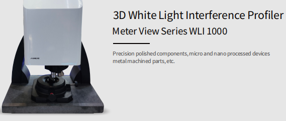
In the field of precision manufacturing, sub-nanometer-level measurement of surface topography has become a core requirement for quality control. White-light interferometry 3D profilometers are redefining the precision boundaries of industrial inspection through their non-contact operation, high accuracy, and three-dimensional imaging capabilities. Technological breakthroughs exemplified by POMEAS white-light interferometry profilometers demonstrate irreplaceable value in sectors such as semiconductors, optical components, and precision machinery.
Non-Contact Measurement

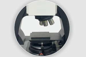
Traditional contact-based probe measurements risk scratching the surfaces of high-value devices, whereas white light interferometry enables non-contact measurement through optical interference principles. POMEAS products employ a modular design combining a spectrographic module with an optical galvanometer, paired with a broad-spectrum white light source, to perform non-destructive inspection of micrometer-scale microstructures. In semiconductor wafer inspection, its sub-nanometer precision effectively captures thin-film thickness deviations and surface defects, preventing wafer damage caused by probe contact. After adopting this technology, an optical component manufacturer achieved surface roughness measurement repeatability of 0.002nm—significantly surpassing the 0.1μm accuracy of traditional methods.
3D Morphological Reconstruction
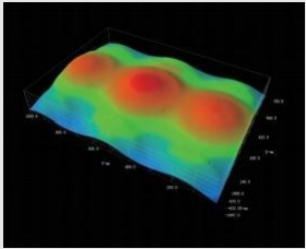
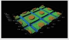
The white light interferometer rapidly reconstructs three-dimensional topography through spectral splitting technology. In Fresnel lens inspection scenarios, POMEAS equipment simultaneously measures curvature radius, profile value (PV), and surface roughness, generating visualizable 3D heatmaps. For specialized optical components like cylindrical and concave mirrors, 3200Hz high-speed sampling and intelligent algorithms instantly capture millions of point cloud data points.
Dynamic Online Detection
To address dynamic inspection demands on high-speed production lines, the POMEAS white light interferometer achieves breakthroughs through multi-station synchronous control and intelligent data processing algorithms. On display panel production lines, it enables 5mm interval sampling of PS adhesive layers on transparent substrates, matching high-speed production requirements. By separating interference signals from the substrate and coating, the system delivers repeatability of 0.015μm with absolute error ≤0.5%. This technology also supports an edge compensation model, precisely capturing thickness variations at the 0.1μm level within 5mm of the coating edge.
POMEAS products achieve full-size coverage from micro-components to large assemblies through multi-view lenses and high-speed digital signal processors. In hardware component inspection, its non-contact measurement eliminates signal distortion caused by material reflectivity variations while adapting to varying surface roughness through an optimized optical system. For aerospace aluminum alloy parts, the equipment simultaneously measures contour, axial curvature, and surface flatness, enabling unattended inspection through automated control systems. In biomedical applications, this technology facilitates rapid assessment of surface coating quality on artificial joints.
Product recommendation
TECHNICAL SOLUTION
MORE+You may also be interested in the following information
FREE CONSULTING SERVICE
Let’s help you to find the right solution for your project!

 ASK POMEAS
  PRICE INQUIRY
  REQUEST DEMO/TEST
  FREE TRIAL UNIT
  ACCURATE SELECTION
 - APPICATION CASE
- RESOURCE CENTER
- DOWNLOAD CENTER
SOLUTIONS SUPPORT
- ZOOM LENS SELECTION TOOL
- TELECENTRIC LENS SELECTION TOOL
- FA LENS SELECTION TOOL
- ZOOM RATIO TABLE
- CERTIFIED MODEL
SELECTION TOOL
- WHY POMEAS
- FAQ
- PRIVACY POLICY
- TERMS OF USE
- DELIVERY & RETURN POLICY
CUSTOMER CARE
 ADDRESS
Add.:No.68, Chongwei Road, Baizhoubian, East district, Dongguan, China, 523000
CONTACT
 Tel:+ 86-0769-2266 0867
 Fax:+ 86-0769-2266 0867
 E-mail:marketing@pomeas.com

Wechat QR code
Software Copyright :2021SR0176001 抄袭必究, 技术支持:誉新源科技