


How is white light interferometry applied to 3D profile measurement?
In the wave of precision manufacturing and scientific research, how can we achieve three-dimensional contour measurement with nanometer-level precision?


The core principle of white light interferometry lies in the phenomenon of light interference. When white light (composite light) illuminates the surface of an object, the reflected light from the surface combines with the reference beam on the detector, forming alternating bright and dark interference fringes. Since white light comprises light of various wavelengths, the distribution of these interference fringes directly correlates with the microscopic topography of the object's surface. By analyzing the phase information of these interference fringes, the system can precisely calculate the height difference at each point on the measured surface, ultimately reconstructing a complete three-dimensional profile.


The advantages of this technology lie in its non-contact nature, high precision, and high resolution. Traditional contact measurement methods may damage precision surfaces, whereas white light interferometry completes measurements through optical scanning, thereby avoiding errors caused by physical contact.
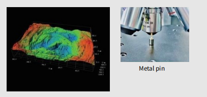
In semiconductor manufacturing, it can detect nanoscale defects on the surface of chips;
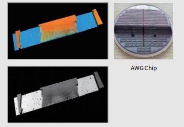
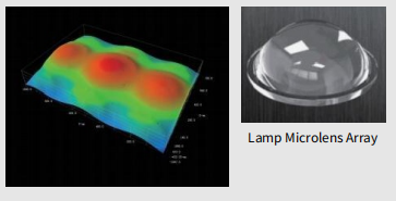
In optical component processing, the surface roughness of lenses can be precisely evaluated.
The POMEAS 3D White Light Interferometric Profiler WLI-1000 is the culmination of this technology.
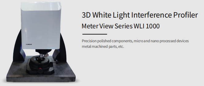
The white light interferometric profilometer employs advanced interferometric objectives and a high-speed data acquisition system, enabling three-dimensional scanning of large surface areas within seconds. Its built-in intelligent algorithms automatically calibrate environmental interference to ensure measurement stability. For instance, in ultra-precision machining applications, POMEAS Instruments has successfully achieved high-precision reproduction of nanoscale step structures with error control within 0.1 nanometers. It also features unique real-time processing capabilities. During measurement, the system simultaneously generates 3D topography maps and surface roughness analysis, enabling users to quickly pinpoint problem areas.
Product recommendation
TECHNICAL SOLUTION
MORE+You may also be interested in the following information
FREE CONSULTING SERVICE
Let’s help you to find the right solution for your project!

 ASK POMEAS
  PRICE INQUIRY
  REQUEST DEMO/TEST
  FREE TRIAL UNIT
  ACCURATE SELECTION
 - APPICATION CASE
- RESOURCE CENTER
- DOWNLOAD CENTER
SOLUTIONS SUPPORT
- ZOOM LENS SELECTION TOOL
- TELECENTRIC LENS SELECTION TOOL
- FA LENS SELECTION TOOL
- ZOOM RATIO TABLE
- CERTIFIED MODEL
SELECTION TOOL
- WHY POMEAS
- FAQ
- PRIVACY POLICY
- TERMS OF USE
- DELIVERY & RETURN POLICY
CUSTOMER CARE
 ADDRESS
Add.:No.68, Chongwei Road, Baizhoubian, East district, Dongguan, China, 523000
CONTACT
 Tel:+ 86-0769-2266 0867
 Fax:+ 86-0769-2266 0867
 E-mail:marketing@pomeas.com

Wechat QR code
Software Copyright :2021SR0176001 抄袭必究, 技术支持:誉新源科技