In today's booming electronics manufacturing industry, PCB boards as the core components of electronic products, its quality inspection is crucial. With unique technical advantages, the zoom navigation lens shows excellent performance in the field of PCB board inspection and becomes a key tool to guarantee the quality of PCB boards.

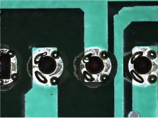
The PCB board integrates intricate circuit lines, tiny electronic components and fine solder joints. Traditional inspection means often face many challenges, manual inspection is not only inefficient, and long time visual fatigue easily lead to leakage and misdetection; ordinary optical inspection equipment in the face of the complex microstructure and macro layout of the PCB board, it is difficult to take into account the overall situation and details, and can not meet the demand for high-precision inspection. The emergence of zoom navigation lens provides an innovative solution to these problems.

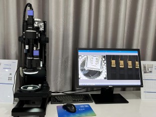
The unique design of the zoom navigation lens, with its two camera ports, allows it to synchronize the global view and the detail view. During PCB inspection, the global field of view can be used first to quickly scan the entire PCB board and quickly locate possible problem areas. For example, macro defects such as obvious line breaks, missing components or offsets can be recognized at a glance. Subsequently, through the detail field of view, without the need for cumbersome lens switching operations, directly penetrate into the suspicious area to carry out a detailed inspection at the microscopic level. It can clearly observe whether the width of the line meets the standard, whether the shape of the solder joints is full and rounded, whether there is any false soldering or continuous soldering phenomenon, as well as whether there is any risk of bending or short-circuiting of tiny components such as chip pins. This seamless inspection method from macro to micro greatly improves the inspection efficiency and accuracy.
The traditional inspection process is time-consuming and has a high defective rate, which seriously affects production efficiency and product quality. After adopting the zoom navigation lens, the inspection speed has been increased by nearly 50%, and the defective outflow rate has been reduced from the original 2% to within 0.5%. This not only effectively reduces production costs, but also greatly enhance the competitiveness of enterprises in the market.
In addition, the zoom navigation lens also has good compatibility, can be easily integrated into the automated inspection line. When working with automated equipment, it can carry out rapid and accurate inspection of PCB boards according to preset procedures, and provide real-time feedback of inspection data to the control system, which facilitates the timely adjustment of production process parameters and further enhances the intelligent level of the production process.
Example diagram of program results:

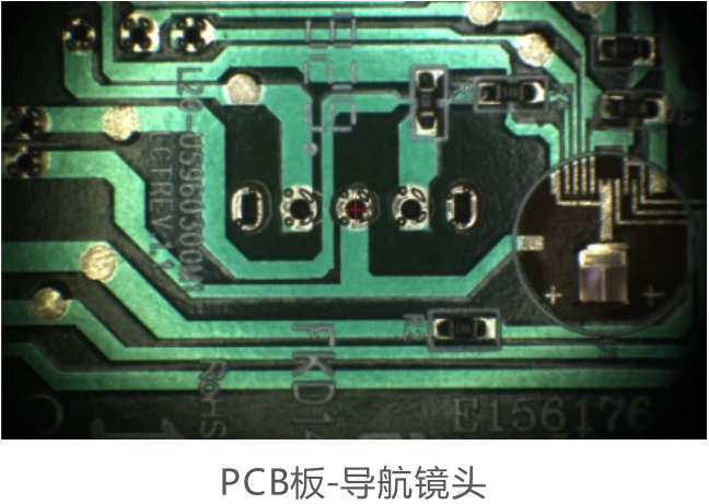
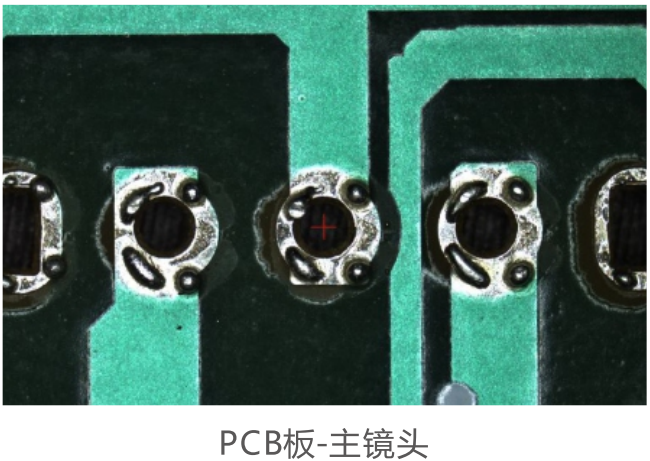

The application of zoom navigation lens in PCB board inspection is undoubtedly an important manifestation of the progress of electronic manufacturing technology. It is efficient, accurate, intelligent characteristics, for the PCB board quality escort, to promote the electronics manufacturing industry towards higher quality, more efficient and effective direction of steady progress.
Product recommendation
TECHNICAL SOLUTION
MORE+You may also be interested in the following information
FREE CONSULTING SERVICE
Let’s help you to find the right solution for your project!

 ASK POMEAS
  PRICE INQUIRY
  REQUEST DEMO/TEST
  FREE TRIAL UNIT
  ACCURATE SELECTION
  ADDRESS
 Tel:+ 86-0769-2266 0867
 Fax:+ 86-0769-2266 0867
 E-mail:marketing@pomeas.com