Electronic Chip Flatness Measurement Background


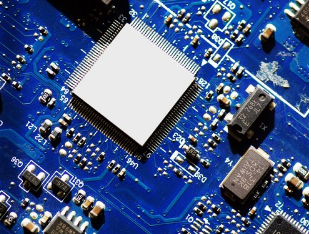
In the manufacturing process of electronic chips, flatness is a crucial quality indicator. With the rapid development of electronic technology, the size of the chip is getting smaller and smaller, the integration degree is getting higher and higher, and the requirements for its flatness are getting more and more strict. For example, the ball grid array package (BGA) chip, its tin ball as a connection point with the circuit board, the flatness of the tin ball is directly related to the reliability of the connection between the chip and the circuit board and electrical performance . If the chip has poor flatness, it may lead to problems such as soldering and short-circuiting during the installation process, which will seriously affect the performance and stability of electronic products and even cause product failure.
Electronic Chip Flatness Measurement Solution: 3D Profilometer


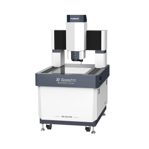
The advantages of POMEAS 3D contouring systems for measuring the flatness of electronic chips include high accuracy, multi-sensor applications, efficient data processing and analysis, flexible measurement methods, and the ability to adapt to a wide range of materials and geometries.
-
High-precision Measurement: POMEAS 3D Profiler's point spectral sensor has high-precision measurement capability, which can accurately obtain the micro-morphological information of the chip surface, providing a reliable data base for flatness measurement. The standard measurement system Metric S322, with servo motor + screw drive, is lightweight and easy to transport and arrange, and at the same time ensures the high accuracy and stability of measurement, and comes standard with a point spectral measurement module, which can be used for scanning measurements, and is highly efficient and comprehensive.
-
Multi-sensor combination applications: POMEAS 3D contour measurement instruments, such as the 3D GMS Pro model, are compatible with multiple types of sensors, including point spectral, line spectral, line laser, surface structured light, and surface interferometric measurement sensors. When measuring the flatness of electronic chips, you can flexibly choose the right sensor or sensor combination according to the specific characteristics of the chip and the measurement needs to realize a more comprehensive and accurate measurement. For example, for chips with complex surface structures, point spectrum sensors and line laser sensors can be combined to give full play to their respective advantages and improve measurement accuracy and efficiency.
-
Efficient data processing and analysis: The profiler is equipped with powerful data processing capabilities and patented algorithms, which can run stably for 7X20H, and its well-designed mainstream machine vision APP, which adopts the OS/APP system architecture, covers the machine vision applications without the need to use a number of different software, which makes it convenient for customers to quickly generate the application that meets their needs. When measuring the flatness of electronic chips, it can quickly and accurately process a large amount of measurement data, extract key feature information, and generate intuitive measurement result reports, which greatly improves the measurement efficiency and work efficiency.
-
Flexible Measurement Mode: Point Spectrum Sensor can adjust the measurement parameters and scanning range according to different measurement scenarios and chip sizes, realizing flatness measurement of various specifications of electronic chips. At the same time, with the gantry-type machine structure and high-precision grinding grade mute rail slider and other mechanical structures, as well as high-speed linear motor-driven multi-axis motion platform, can realize fast and stable measurement, the maximum measuring stroke up to 3.6 meters, to meet the different production lines on the electronic chip flatness inspection needs!
Product recommendation
TECHNICAL SOLUTION
MORE+You may also be interested in the following information
FREE CONSULTING SERVICE
Let’s help you to find the right solution for your project!


 ASK POMEAS
  PRICE INQUIRY
  REQUEST DEMO/TEST
  FREE TRIAL UNIT
  ACCURATE SELECTION
  ADDRESS
 Tel:+ 86-0769-2266 0867
 Fax:+ 86-0769-2266 0867
 E-mail:marketing@pomeas.com
