Laser autofocus microscopy in the semiconductor industry case study: Wafer focusing
With the rapid development of semiconductor technology, the quality and performance of wafers, as the basic material of semiconductor chips, are crucial to the entire chip manufacturing process. Laser autofocus microscopy, with its high precision, high efficiency and intelligent features, plays an increasingly important role in wafer focusing in the semiconductor industry.


In the semiconductor manufacturing process, defect detection and microstructure analysis on the wafer surface are critical steps to ensure chip quality. Traditional inspection means often have problems such as lack of precision, low efficiency and susceptibility to human factors. By utilizing the self-focusing property of the laser beam, laser autofocus microscopy technology realizes precise focusing and efficient scanning of the wafer surface, which greatly improves the accuracy and efficiency of inspection.


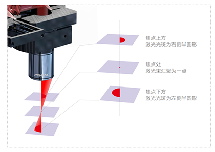
Principles of laser focusing microscopy systems:
In the semiconductor manufacturing process, defect detection and microstructure analysis on the wafer surface are critical steps to ensure chip quality. Traditional inspection means often have problems such as lack of precision, low efficiency and susceptibility to human factors. By utilizing the self-focusing property of the laser beam, laser autofocus microscopy technology realizes precise focusing and efficient scanning of the wafer surface, which greatly improves the accuracy and efficiency of inspection.


Application Advantage:
1. Improve inspection accuracy: laser autofocus microscopy technology can achieve micron or even nanometer focusing accuracy, ensuring accurate detection of wafer surface defects and fine structure, providing a strong guarantee for chip quality.
2. Enhance inspection efficiency: The technology has a fast and accurate autofocus function, which reduces the time and error of manual operation and greatly improves the productivity of wafer inspection.
3. Reduce human error: The laser autofocus microscope system does not depend on the operator's skills and experience, reducing the occurrence of human error and improving the reliability and stability of the inspection.
4. Non-destructive inspection: The use of non-contact inspection methods will not cause damage to the wafer, ensuring the integrity and reliability of the wafer.
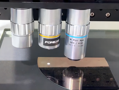
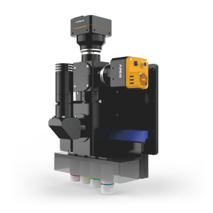
The automated and highly accurate detection of defects and microstructures on wafer surfaces has been realized through the introduction of the advanced POMEAS laser autofocus microscopy system. In practical application, the POMEAS AFM system is able to quickly and accurately identify scratches, stains, cracks and other defects on the wafer surface, as well as analyze the fine structure in detail. At the same time, the system is also able to monitor the accuracy and consistency of the pattern during the lithography process in real time to ensure the quality of lithography. The realization of these functions not only improves the efficiency and precision of wafer inspection, but also significantly reduces the rate of defective products, bringing significant economic benefits to the enterprise.
Product recommendation
TECHNICAL SOLUTION
MORE+You may also be interested in the following information
FREE CONSULTING SERVICE
Let’s help you to find the right solution for your project!


 ASK POMEAS
  PRICE INQUIRY
  REQUEST DEMO/TEST
  FREE TRIAL UNIT
  ACCURATE SELECTION
  ADDRESS
 Tel:+ 86-0769-2266 0867
 Fax:+ 86-0769-2266 0867
 E-mail:marketing@pomeas.com
