Measurement semiconductor industry background:
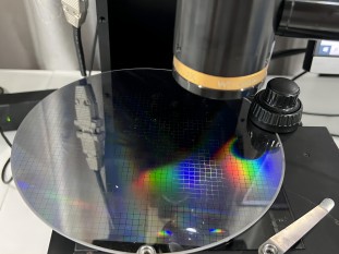
As the cornerstone of modern electronic technology, the quality and performance of semiconductor products directly affect the development of the entire electronics industry. With the rapid development of the Internet of Things, artificial intelligence, 5G communications and other emerging technologies, the precision, stability and reliability of semiconductor products are increasingly demanding. Precise measurement and testing in the semiconductor manufacturing process is a key link to ensure product quality. Especially in the stages of chip manufacturing, packaging and testing, the precise measurement of tiny size, shape and surface defects is particularly important.


Characteristics of telecentric lenses:
1、Extremely small object telecentricity error: No matter how the distance of the object from the lens changes, the size of the image remains basically constant, effectively eliminating the imaging size error caused by changes in object distance. This feature is particularly important in semiconductor measurement to ensure the accuracy and consistency of measurement results.
2、High resolution: Telecentric lenses capture the finest details of an object, providing clear, sharp images. In semiconductor manufacturing, this helps to detect tiny lines, structures and defects on the chip, guaranteeing high performance and stability.
3、Low distortion: During the imaging process, the telecentric lens minimizes distortion and warping of the image, ensuring that the resulting image truly and accurately reflects the actual shape of the object. This is critical for precise size and shape measurements in semiconductor metrology.
4、Large Depth of Field: Telecentric lenses typically have a large depth of field, which allows the entire object to be clearly imaged over a range of object distances. In semiconductor measurements, this helps to observe and analyze multiple layers and areas on a chip simultaneously, improving measurement efficiency.
5、Good light uniformity: The telecentric lens provides relatively uniform light effects over the entire imaging area, avoiding image quality degradation due to uneven light. This is important for image processing and analysis in semiconductor measurements.


Telecentric lens measurement semiconductor program:
1. Chip Pin Spacing Measurement: Semiconductor chips usually have very small pin spacing, which requires high measurement accuracy. With its high resolution and low distortion, telecentric lenses can accurately measure the pin spacing to ensure the quality and reliability of the chip.
2. Chip Surface Defect Detection: Scratches, cracks, contamination and other defects may exist on the surface of the chip, and these defects will affect the performance and stability of the chip. Telecentric lenses help inspectors quickly and accurately find these defects by providing clear, sharp images and make timely repairs or replacements.
3. Package testing: In the semiconductor packaging process, the package needs to be measured and inspected accurately. Telecentric lenses ensure that clear visual images are obtained simultaneously at different working distances, improving the efficiency and accuracy of package testing.
4. 3D Measurement and Reverse Engineering: 3D measurement and reverse engineering are indispensable in the design and manufacturing of semiconductor products. Telecentric lenses can obtain clear images of multiple layers of an object at once, providing reliable data support for 3D modeling and reverse engineering.
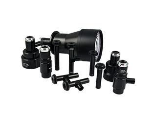
Product recommendation
TECHNICAL SOLUTION
MORE+You may also be interested in the following information
FREE CONSULTING SERVICE
Let’s help you to find the right solution for your project!


 ASK POMEAS
  PRICE INQUIRY
  REQUEST DEMO/TEST
  FREE TRIAL UNIT
  ACCURATE SELECTION
  ADDRESS
 Tel:+ 86-0769-2266 0867
 Fax:+ 86-0769-2266 0867
 E-mail:marketing@pomeas.com
