Spectral Alignment Vision Measurement Solution for Wafer Inspection
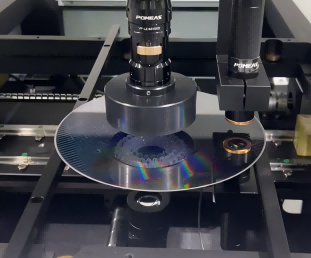
In the semiconductor industry, the inspection of wafers is a critical step in ensuring chip quality and performance. With the development of technology, there is an increasing demand for wafer inspection accuracy and efficiency. In this paper, we will introduce an innovative spectral alignment vision measurement solution that uses the features of POMEAS products to provide an efficient and accurate solution for wafer inspection.


Product Features Explained:
1. Non-contact design of the alignment structure
① POMEAS spectral alignment vision measurement solution adopts a unique alignment structure design to achieve non-contact measurement.
② The non-contact design of the alignment structure disregards the material of the product and enables accurate measurement of the wafer, avoiding any damage or contamination that may be caused by contact and ensuring the reliability and repeatability of the measurement.
2. Fast positioning of image measurement components and spectra
① The combination of image measurement components and spectroscopy technology enables rapid positioning of wafers.
② The rapid positioning technology not only improves the measurement efficiency, but also ensures the accuracy of the wafer position during the measurement process, laying a solid foundation for the subsequent precision measurement.
3. 3-axis non-stop data acquisition
① POMEAS measurement solution supports 3-axis non-stop data acquisition, which means that no need to stop the equipment during the measurement process to achieve rapid measurement of wafer flatness, thickness and other parameters.
② The continuous measurement method greatly improves productivity and meets the high efficiency requirements of modern semiconductor manufacturing.
4. PMS-SFS-8012 Point Spectrum Sensor
① Using PMS-SFS-8012 point spectral sensor, this solution can achieve accurate and stable measurement with an accuracy of up to 1μm.
② The high-precision sensor provides accurate measurement results for wafer size and shape, ensuring the quality and performance of semiconductor products.
5. 3DOS Measurement System
① Equipped with a self-made 3DOS measurement system, this solution supports visual and multi-sensor composite operation, providing an easy-to-use and convenient operation interface.
② 3DOS measurement system not only simplifies the measurement process, but also improves the flexibility and accuracy of the measurement, enabling operators to quickly get started and efficiently complete the measurement tasks.
POMEAS Spectral Alignment Vision Measurement solution brings a revolutionary technological breakthrough to wafer inspection. With its non-contact design, fast positioning, 3-axis non-stop data acquisition, high-precision sensors and easy-to-use measurement system, the solution not only improves the accuracy and efficiency of wafer inspection, but also reduces production costs and meets the semiconductor industry's stringent requirements for high-precision inspection.
Product recommendation
TECHNICAL SOLUTION
MORE+You may also be interested in the following information
FREE CONSULTING SERVICE
Let’s help you to find the right solution for your project!


 ASK POMEAS
  PRICE INQUIRY
  REQUEST DEMO/TEST
  FREE TRIAL UNIT
  ACCURATE SELECTION
  ADDRESS
 Tel:+ 86-0769-2266 0867
 Fax:+ 86-0769-2266 0867
 E-mail:marketing@pomeas.com
