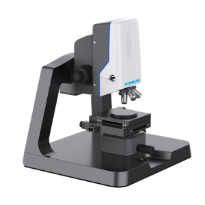
White light interferometric 3D profilometer, the specialist for optical surface measurements
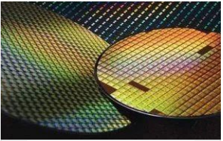
With the development of semiconductor technology, the requirements for wafer surface quality are getting higher and higher. While conventional contact measurement methods may cause damage to the wafer surface, the POMEAS White Light Interference 3D Profiler utilizes non-contact measurement technology to non-destructively inspect the surface condition, thickness variation and shape accuracy of wafers.
Principle of operation of the POMEAS White Light Interference 3D Profiler:


Based on the principle of white light interference, the POMEAS White Light Interference 3D Profiler projects a broadband light source onto the wafer surface and utilizes the reflected light on the wafer surface to interfere with the reference light to form interference patterns. By analyzing these interference patterns, the 3D topography information of the wafer surface can be obtained.
Technological Advantage:
Non-contact measurement: avoids the risk of damage to the wafer surface.
High resolution: capable of detecting surface changes down to the nanometer scale.
Fast measurement: automated measurement process greatly reduces inspection time.
Multi-parameter inspection: not only measures surface topography, but also evaluates thickness uniformity and shape accuracy.
Applications:
Surface Defect Detection: Identify tiny defects and particles on the wafer surface.
Thickness Consistency Assessment: Ensure uniform thickness distribution of wafers to avoid deviation during production.
Shape Accuracy Measurement: Accurately measure the curvature and flatness of wafers to ensure the accuracy of subsequent processing.

With its excellent performance and reliability, POMEAS White Light Interference 3D Profiler has become an important tool for wafer inspection in the semiconductor industry. It not only improves the inspection efficiency, but also ensures the quality and performance of the wafers, providing strong support for the further development of semiconductor manufacturing.
Product recommendation
TECHNICAL SOLUTION
MORE+You may also be interested in the following information
FREE CONSULTING SERVICE
Let’s help you to find the right solution for your project!

- APPICATION CASE
- RESOURCE CENTER
- DOWNLOAD CENTER
SOLUTIONS SUPPORT
- ZOOM LENS SELECTION TOOL
- TELECENTRIC LENS SELECTION TOOL
- FA LENS SELECTION TOOL
- ZOOM RATIO TABLE
- CERTIFIED MODEL
SELECTION TOOL
- WHY POMEAS
- FAQ
- PRIVACY POLICY
- TERMS OF USE
- DELIVERY & RETURN POLICY
CUSTOMER CARE
 ADDRESS
Add.:No.68, Chongwei Road, Baizhoubian, East district, Dongguan, China, 523000
CONTACT
 Tel:+ 86-0769-2266 0867
 Fax:+ 86-0769-2266 0867
 E-mail:marketing@pomeas.com

Wechat QR code

 ASK POMEAS
  PRICE INQUIRY
  REQUEST DEMO/TEST
  FREE TRIAL UNIT
  ACCURATE SELECTION