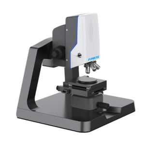
White light interference profilometer is a high-precision optical measuring instrument, mainly used for sub-nanometer non-contact measurement of various precision devices and material surfaces.
Fundamentals:
The white light interference profiler is based on the principle of white light interference technology, and the reference and detection optical paths are formed by different optical components. The illumination beam is divided into two beams by a half-reflective and half-transmissive beamsplitter, which are projected onto the sample surface and the reference mirror surface respectively. The two beams of light reflected from the two surfaces pass through the beamsplitter again and are synthesized into a single beam of light, which is used by the imaging system to form two superimposed images on the light-sensitive surface of the CCD camera. As the two beams of light interfere with each other, light and dark interference fringes are observed on the sensitive surface of the CCD camera. The brightness of the interference fringes depends on the optical range difference between the two beams of light, according to the brightness of the white light interference fringes as well as the location of the interference fringes, the relative height of the sample can be resolved, thus realizing the precise measurement of the sample surface topography.


Product Features:
1. High precision: The white light interference profiler has sub-nanometer display accuracy and can measure the sample surface with high precision.
2. Non-contact measurement: non-contact measurement method is adopted to avoid the damage that traditional contact measurement may cause to the sample surface.
3. Fast measurement: fast measurement speed, able to complete the measurement of a large number of samples in a short period of time.
4. Multi-parameter Measurement: It can automatically focus on the measurement workpiece and obtain more than one hundred parameters such as 2D and 3D surface roughness and contour.
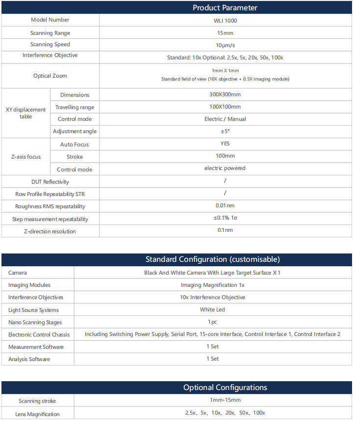
Technical parameters:

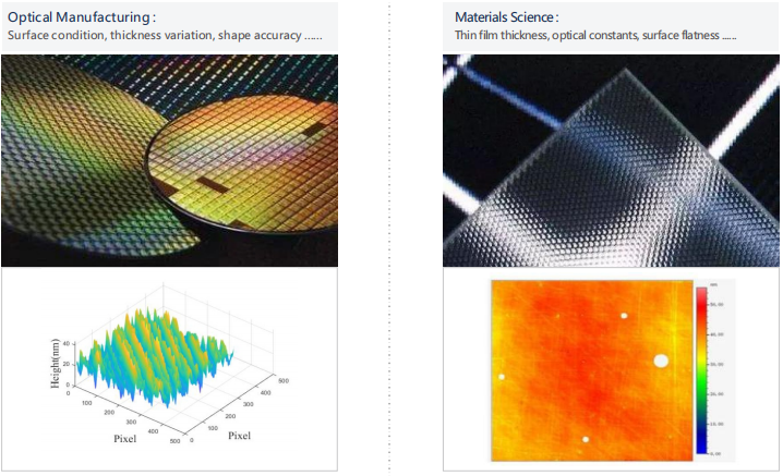
Areas of application:
Material Science: Used to measure and analyze the flatness, roughness, corrugation, surface profile, surface defects, etc. of various material surfaces.
Optoelectronics: Used to measure the thickness of thin films, coatings, and the quality of optical films, etc.
Microelectronics: for microelectronic surface analysis and MEMS characterization, etc.
Mechanical manufacturing: contour, axial curvature, surface flatness

Product recommendation
TECHNICAL SOLUTION
MORE+You may also be interested in the following information
FREE CONSULTING SERVICE
Let’s help you to find the right solution for your project!

- APPICATION CASE
- RESOURCE CENTER
- DOWNLOAD CENTER
SOLUTIONS SUPPORT
- ZOOM LENS SELECTION TOOL
- TELECENTRIC LENS SELECTION TOOL
- FA LENS SELECTION TOOL
- ZOOM RATIO TABLE
- CERTIFIED MODEL
SELECTION TOOL
- WHY POMEAS
- FAQ
- PRIVACY POLICY
- TERMS OF USE
- DELIVERY & RETURN POLICY
CUSTOMER CARE
 ADDRESS
Add.:No.68, Chongwei Road, Baizhoubian, East district, Dongguan, China, 523000
CONTACT
 Tel:+ 86-0769-2266 0867
 Fax:+ 86-0769-2266 0867
 E-mail:marketing@pomeas.com

Wechat QR code

 ASK POMEAS
  PRICE INQUIRY
  REQUEST DEMO/TEST
  FREE TRIAL UNIT
  ACCURATE SELECTION