Application of White Light Interference 3D Profiler in Chip Inspection
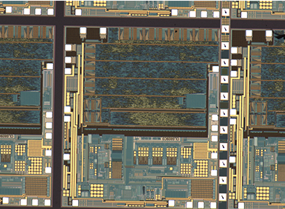
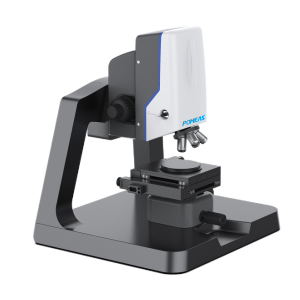
In today's highly evolving chip industry, precision and quality control of chips is crucial, and white light interferometric 3D profilers are becoming an indispensable and critical tool in chip inspection.


White light interference 3D profilers play an important role in wafer production:
1、Measurement of wafer surface roughness: able to detect the microscopic unevenness of the wafer surface with very high precision and resolution, providing accurate surface base data for subsequent processes. Through the accurate measurement to the nanometer level, to ensure that the wafer surface to meet the requirements of further processing.
2、detection of wafer flatness (warpage): can quickly and comprehensively scan the entire wafer surface, to build a precise three-dimensional morphology, accurately reflecting the degree of warpage of the wafer everywhere, which is of great significance for the accurate stacking of multi-layer chip structures and subsequent lithography and other processes.
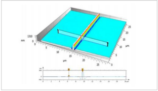
3、chip lithography process: can be photolithography after the pattern structure of the microscopic topography detection, such as the height of the line, the depth of the groove, etc.. Its non-contact measurement characteristics to avoid damage to the fine lithographic structure and pollution, to ensure the integrity of the lithographic structure.
4、when the wafer thinning process: can real-time measurement of the thickness change after thinning, to ensure that the wafer in the thinning process to meet the design thickness standards, and again on the thinned wafer surface roughness assessment, to ensure that the thinning process will not be introduced to the new surface defects and roughness is too large problem.
5、for the chip cutting groove: can accurately measure the groove depth, groove width and chipping and other morphological characteristics, for optimizing the cutting process parameters, improve the quality of chip cutting and yield has an important guiding significance.
6、detecting the surface flatness and microscopic morphology of the packaging structure: especially in advanced packaging technology, high-precision morphology analysis of the interface between different materials and structures to ensure the reliability and stability of the package.
Unique Advantages of White Light Interference 3D Profilers


(1) High-precision measurement: with nanometer or even sub-nanometer longitudinal resolution24, it can accurately capture extremely small morphological changes and dimensional differences on the chip surface.
(2) Non-contact measurement: no damage or risk of contamination to the chip, keeping the physical state of the chip intact.
(3) Rapid imaging and automated analysis: imaging and automatically analyzing the results within a few seconds2, greatly improving the detection efficiency and adapting to the rhythm of large-scale chip production.
(4) Powerful software analysis function: it can carry out a variety of analyses including roughness analysis, geometric profile analysis, structural analysis, frequency analysis, functional analysis and so on.

White light interference 3D profilometer for chip manufacturing from design and development to the whole process of large-scale production to provide a reliable, accurate and efficient means of inspection, and strongly promote the chip industry continues to develop in the direction of smaller size, higher performance and higher yield.
Product recommendation
TECHNICAL SOLUTION
MORE+You may also be interested in the following information
FREE CONSULTING SERVICE
Let’s help you to find the right solution for your project!


 ASK POMEAS
  PRICE INQUIRY
  REQUEST DEMO/TEST
  FREE TRIAL UNIT
  ACCURATE SELECTION
  ADDRESS
 Tel:+ 86-0769-2266 0867
 Fax:+ 86-0769-2266 0867
 E-mail:marketing@pomeas.com
