


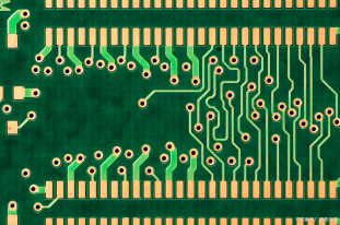
With the rapid development of the electronics industry, PCB (Printed Circuit Board) as the carrier of the electrical connection of electronic components, its manufacturing quality requirements are increasingly high. The development trend of high precision, high density and high reliability makes the inspection of PCB especially important. In this context, telecentric lens, as an advanced visual inspection tool, its application in PCB printing is becoming more and more widespread, providing a new and innovative solution for PCB inspection.
Principle of operation and characteristics of telecentric lenses:
Telecentric lenses are designed to correct the parallax of traditional industrial lenses, which is characterized by the fact that the image magnification does not change within a certain object distance. This feature makes the telecentric lens has a unique advantage in PCB inspection. Specifically, the telecentric lens using telecentric optical path design, divided into object-side telecentric optical path and image-side telecentric optical path. Object-side telecentric optical path can eliminate the object side due to inaccurate focus brought about by the reading error, while the image-side telecentric optical path can eliminate the image side of the focus is not allowed to introduce the measurement error. The two-side telecentric optical path combines the dual role of object-side and image-side telecentricity, making the detection more accurate and reliable.
Detection Program:

PCB Visual Alignment System
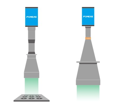
PCB vision alignment system is a key technology to realize automatic PCB scanning and positioning. In this system, the telecentric lens, as a key component, can image the target on the photosensitive surface of the image sensor. By using a webcam and POMEAS high depth-of-field telecentric lens, it can ensure that the product can be imaged clearly up to a certain height, with stable and reliable performance. This solution not only improves inspection accuracy, but also greatly increases productivity.
High Precision Defect Detection
Defect detection is a crucial part of the PCB manufacturing process. The high resolution and low distortion characteristics of telecentric lenses make it possible to accurately capture minute defects on circuit boards, such as cracks, scratches, stains, etc.. By combining with image processing software, automatic identification and classification of defects can be realized, thus improving inspection efficiency and accuracy.
Component Position and Dimension Inspection
On PCBs, the positional and dimensional accuracy of electronic components has a significant impact on product performance. Telecentric lenses ensure that the image magnification remains constant during the measurement process, enabling precise measurement of component position and dimensions. This solution not only improves measurement accuracy, but also helps to optimize production processes and improve product quality.

As an advanced visual inspection tool, POMEAS high-resolution telecentric lenses have a wide range of applications in the PCB printing field. By combining PCB vision alignment system, high-precision defect detection and component position and size inspection solutions, accurate control and efficient inspection of the whole PCB manufacturing process can be realized.
Product recommendation
TECHNICAL SOLUTION
MORE+You may also be interested in the following information
FREE CONSULTING SERVICE
Let’s help you to find the right solution for your project!

 ASK POMEAS
  PRICE INQUIRY
  REQUEST DEMO/TEST
  FREE TRIAL UNIT
  ACCURATE SELECTION
 - APPICATION CASE
- RESOURCE CENTER
- DOWNLOAD CENTER
SOLUTIONS SUPPORT
- ZOOM LENS SELECTION TOOL
- TELECENTRIC LENS SELECTION TOOL
- FA LENS SELECTION TOOL
- ZOOM RATIO TABLE
- CERTIFIED MODEL
SELECTION TOOL
- WHY POMEAS
- FAQ
- PRIVACY POLICY
- TERMS OF USE
- DELIVERY & RETURN POLICY
CUSTOMER CARE
 ADDRESS
Add.:No.68, Chongwei Road, Baizhoubian, East district, Dongguan, China, 523000
CONTACT
 Tel:+ 86-0769-2266 0867
 Fax:+ 86-0769-2266 0867
 E-mail:marketing@pomeas.com

Wechat QR code
Software Copyright :2021SR0176001 抄袭必究, 技术支持:誉新源科技