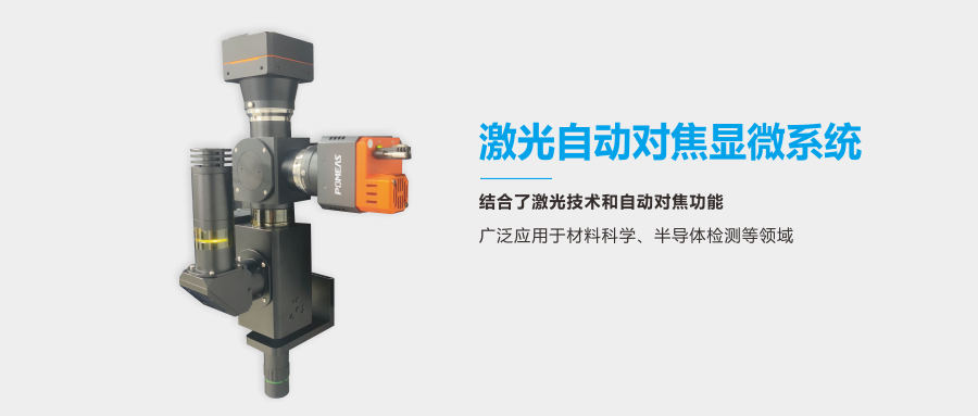
The dual-camera design of the laser autofocus microscope system consists of a laser source, a microscope head, an autofocus mechanism, and two high-resolution cameras. The laser source is used to provide a high brightness, high monochromatic light source to enhance the contrast and clarity of the image. The microscope head is used to magnify the details of the sample under observation, while the autofocus mechanism ensures that the lens is always at an optimal distance from the sample to obtain the clearest image. Two cameras capture images from different angles or at different magnifications to provide more comprehensive and accurate observations.


Program Strengths:
1、High-precision focusing: The auto-focusing mechanism can quickly and accurately adjust the distance between the lens and the sample to ensure that the image is always in the clearest state.
2, high-resolution imaging: two high-resolution cameras can capture the minute details of the sample, providing researchers with rich data support.
3、Multi-angle observation: The dual-camera design allows the sample to be observed from different angles, which helps to discover hidden features or defects in the sample.
4、Real-time dynamic monitoring: The system is able to monitor changes in the sample in real time, providing real-time feedback for researchers.
Areas of application:
1、Materials science: In the field of materials science, the system can be used to observe the microstructure, phase transition process and interface behavior of materials. Through high-resolution imaging and multi-angle observation, researchers can gain an in-depth understanding of the nature and behavior of materials, providing strong support for material design and optimization.
2、Semiconductor Inspection: In the semiconductor manufacturing process, the system can be used to detect defects on the chip surface, pollution and circuit layout. Through real-time dynamic monitoring and high-precision focusing, the system is able to detect and repair problems in time, improving the quality and reliability of semiconductor products.
3, biological research: in the field of biology, the system can be used to observe the structure and function of cells, tissues and biological macromolecules. Through high-resolution imaging and multi-angle observation, researchers can gain an in-depth understanding of the physiological and pathological processes of organisms, providing important support for biomedical research.
4、Nanotechnology: In the field of nanotechnology, the system can be used to observe the morphology and size of nanomaterials as well as their interaction with other materials. This information is important for the preparation, characterization and application of nanomaterials.
The dual-camera design of POMEAS laser autofocus microscope combines laser technology and autofocus function, providing powerful technical support for material science, semiconductor inspection, etc. The system features high-precision focusing, high-resolution imaging, multi-angle observation and real-time dynamic monitoring. The system features high-precision focusing, high-resolution imaging, multi-angle observation, and real-time dynamic monitoring to meet the inspection needs of different fields.
Product recommendation
TECHNICAL SOLUTION
MORE+You may also be interested in the following information
FREE CONSULTING SERVICE
Let’s help you to find the right solution for your project!


 ASK POMEAS
  PRICE INQUIRY
  REQUEST DEMO/TEST
  FREE TRIAL UNIT
  ACCURATE SELECTION
  ADDRESS
 Tel:+ 86-0769-2266 0867
 Fax:+ 86-0769-2266 0867
 E-mail:marketing@pomeas.com
