


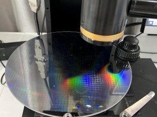
In semiconductor manufacturing, observation and inspection of wafers is a critical step in ensuring product quality and performance. With the continuous progress of technology, the requirements for observation equipment are also increasing. Among the many observation techniques, laser autofocus microscope has become the preferred tool for wafer observation due to its unique advantages.

Fundamentals of laser autofocus microscopy:
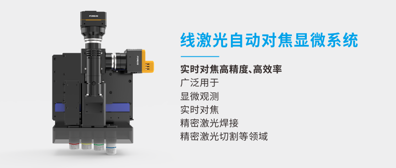
The laser autofocus microscope combines laser technology and autofocus functionality to achieve precise focus control through the self-focusing properties of the laser beam. During the observation process, the laser beam passes through an illuminating pinhole to form a point light source that scans the wafer surface. The irradiated point is imaged at the probe pinhole and received point by point or line by line by the light point multiplier tube or cold electrocoupler device behind the probe pinhole, which rapidly forms a fluorescent image on the computer monitor screen. By precisely controlling the self-focusing and scattering points of the laser beam, the system can realize the focus adjustment of the wafer surface, thus obtaining clearer microscopic images.
Advantages of laser autofocus microscopy:

1, high-precision detection: laser autofocus microscopy system can achieve micron-level detection accuracy to meet the needs of high-precision experiments and inspection. This is crucial for observing the fine structure and defects of wafers.
2, non-contact detection: the system adopts non-contact detection, avoiding the pollution and damage that may be introduced in the traditional detection methods, to ensure the integrity and safety of the wafer.
3, rapid detection: the system has a fast auto-focus function, can complete a large number of wafers in a short period of time to complete the task of inspection, improve production efficiency and inspection efficiency.
4, visualization of inspection results: inspection results can be displayed in the form of images or video, making the inspection process more intuitive and easy to understand. This enables researchers and technicians to identify and solve problems more quickly and accurately.
Application of laser autofocus microscopy system in wafer observation:
① Wafer Surface Defect Detection: The laser autofocus microscope system can quickly and accurately identify defects on the wafer surface, such as scratches, stains, cracks, etc., to provide strong support for quality control in the production process.
② Photolithography monitoring: Photolithography is a critical step in semiconductor manufacturing, and its accuracy directly affects chip performance. The laser autofocus microscope system can monitor the accuracy and consistency of the pattern during the lithography process in real time to ensure the quality of lithography.
③ Observation of internal chip structure and devices: The laser autofocus microscope system has high resolution and high sensitivity, and can be used to observe the structure and devices inside the chip. By adjusting the focus, the system can clearly display the circuit layout and transistor structure inside the chip, providing researchers with a powerful analytical tool.
With the continuous development of semiconductor technology, laser autofocus microscopy systems will continue to play an important role in providing a strong guarantee for the quality and performance of semiconductor chips. For the semiconductor manufacturing industry, choosing a laser autofocus microscope as an observation tool is undoubtedly a wise choice.
Product recommendation
TECHNICAL SOLUTION
MORE+You may also be interested in the following information
FREE CONSULTING SERVICE
Let’s help you to find the right solution for your project!

 ASK POMEAS
  PRICE INQUIRY
  REQUEST DEMO/TEST
  FREE TRIAL UNIT
  ACCURATE SELECTION
 - APPICATION CASE
- RESOURCE CENTER
- DOWNLOAD CENTER
SOLUTIONS SUPPORT
- ZOOM LENS SELECTION TOOL
- TELECENTRIC LENS SELECTION TOOL
- FA LENS SELECTION TOOL
- ZOOM RATIO TABLE
- CERTIFIED MODEL
SELECTION TOOL
- WHY POMEAS
- FAQ
- PRIVACY POLICY
- TERMS OF USE
- DELIVERY & RETURN POLICY
CUSTOMER CARE
 ADDRESS
Add.:No.68, Chongwei Road, Baizhoubian, East district, Dongguan, China, 523000
CONTACT
 Tel:+ 86-0769-2266 0867
 Fax:+ 86-0769-2266 0867
 E-mail:marketing@pomeas.com

Wechat QR code
Software Copyright :2021SR0176001 抄袭必究, 技术支持:誉新源科技