


4K zoom lenses have revolutionized the semiconductor manufacturing industry by demonstrating significant advantages in wafer defect inspection. With its high resolution, large field of view, fast inspection speed and precise measurement capability, this lens has become the ideal choice in the field of wafer defect inspection.

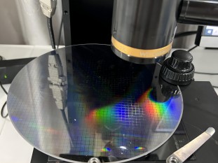
High Resolution: The high resolution nature of the 4K zoom lens allows it to capture extremely small defects on the wafer surface. These defects may include dust residue, oxidation, scratches, and linear defects, which can have a serious impact on the performance and reliability of the wafer. Through the precise identification of the 4K zoom lens, defects can be detected and rejected in a timely manner, ensuring stable product quality.
Large field of view: The large field of view of the 4K zoom lens makes the inspection process more efficient. Compared to traditional inspection equipment, it is able to complete a larger scanning area in a shorter period of time, which greatly improves the inspection efficiency. This is critical for the semiconductor manufacturing industry, where wafers are produced on a large scale and inspection tasks need to be completed quickly and accurately.
Fast Inspection: The fast inspection speed of the 4K zoom lens is also a major advantage. It is able to fully inspect wafers in a very short period of time, detecting potential problems in time and reducing downtime and cost losses in the production process. At the same time, due to the fast inspection speed, it can also improve the overall efficiency of the production line, creating more value for the enterprise.
Accurate Measurement: The precise measurement capability of the 4K zoom lens is also an indispensable advantage in wafer defect detection. It can accurately measure the size and location of various defects on the wafer surface, providing strong data support for subsequent repair and improvement. This precise measurement capability makes wafer defect inspection more scientific, objective and reliable.

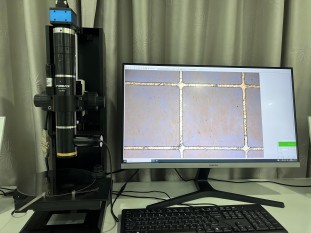
The 4K zoom lens offers significant advantages in wafer defect inspection, including high resolution, large field of view, fast inspection speed, and precise measurement capability. These advantages make it an indispensable and important tool in the semiconductor manufacturing industry, bringing significant contributions to improving product quality, increasing production efficiency and reducing costs.
Product recommendation
TECHNICAL SOLUTION
MORE+You may also be interested in the following information
FREE CONSULTING SERVICE
Let’s help you to find the right solution for your project!

 ASK POMEAS
  PRICE INQUIRY
  REQUEST DEMO/TEST
  FREE TRIAL UNIT
  ACCURATE SELECTION
 - APPICATION CASE
- RESOURCE CENTER
- DOWNLOAD CENTER
SOLUTIONS SUPPORT
- ZOOM LENS SELECTION TOOL
- TELECENTRIC LENS SELECTION TOOL
- FA LENS SELECTION TOOL
- ZOOM RATIO TABLE
- CERTIFIED MODEL
SELECTION TOOL
- WHY POMEAS
- FAQ
- PRIVACY POLICY
- TERMS OF USE
- DELIVERY & RETURN POLICY
CUSTOMER CARE
 ADDRESS
Add.:No.68, Chongwei Road, Baizhoubian, East district, Dongguan, China, 523000
CONTACT
 Tel:+ 86-0769-2266 0867
 Fax:+ 86-0769-2266 0867
 E-mail:marketing@pomeas.com

Wechat QR code
Software Copyright :2021SR0176001 抄袭必究, 技术支持:誉新源科技