Advantages of laser autofocus microscopy for semiconductor chip inspection applications
With the rapid development of science and technology, semiconductor chips have become an indispensable key element of modern society. In order to ensure the performance and quality of the chip, high-precision inspection technology is particularly important. As an advanced inspection technology, laser autofocus microscopy system plays an important role in semiconductor chip inspection.
Detection principle of laser autofocus microscopy system:

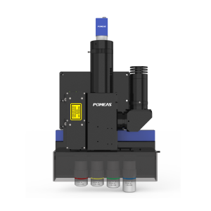
Laser autofocus microscopy systems utilize the self-focusing properties of the laser beam to achieve precise focus control. During the inspection process, the laser beam passes through the illumination pinhole to form a point light source that scans the surface of the semiconductor chip. The irradiated point is imaged at the detection pinhole and received point by point or line by line by the light point multiplier tube or cold electrocoupler device behind the detection pinhole, which rapidly forms a fluorescent image on the computer monitor screen. By precisely controlling the self-focusing and scattering points of the laser beam, the system can realize focus adjustment on the surface of the semiconductor chip, thus obtaining clearer microscopic images.
Application of laser autofocus microscopy system in semiconductor chip inspection


Semiconductor Chip
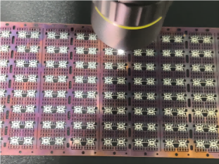
1, wafer inspection: In the semiconductor manufacturing process, defect detection and fine structure analysis of the wafer surface is crucial. Laser autofocus microscopy system can quickly and accurately identify defects on the wafer surface, such as scratches, stains, cracks, etc., and conduct fine analysis of the fine structure to ensure the quality of the wafer.
2, photolithography: photolithography is a key step in semiconductor manufacturing, and its accuracy directly affects the performance of the chip. The laser auto-focus microscope system can monitor the accuracy and consistency of the pattern in the photolithography process in real time to ensure the quality of photolithography.
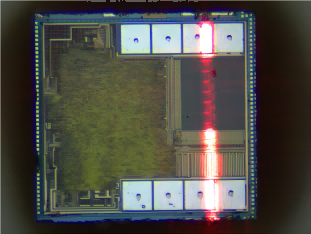
3, the internal structure of the chip and device observation: laser autofocus microscope system with high resolution and high sensitivity, can be used to observe the internal structure of the chip and device. By adjusting the focus, the system can clearly display the circuit layout and transistor structure inside the chip, providing researchers with powerful analytical tools.


Focusing Example
Advantages of laser autofocus microscope system in semiconductor chip inspection
1, improve productivity: laser autofocus microscope system has a fast and accurate autofocus function, reducing the time and error of manual operation, thus improving the productivity of semiconductor chip inspection.
2, improve detection accuracy: laser autofocus microscope system can realize precise focus control, to ensure that the semiconductor chip inspection process focus accurately, so as to provide a clearer, more detailed image or data, help to improve the detection accuracy.
3, reduce human error: laser autofocus microscopy system does not depend on the operator's skills and experience, reducing the occurrence of human error, improve the reliability and stability of detection.
4, non-destructive detection: laser autofocus microscopy system adopts non-contact detection, will not cause damage to the semiconductor chip, to ensure the integrity and reliability of the chip.
As an advanced inspection technology, laser autofocus microscopy system has a wide range of applications and significant advantages in semiconductor chip inspection. With the continuous development of semiconductor technology, laser autofocus microscopy system will continue to play an important role in providing a strong guarantee for the quality and performance of semiconductor chips.
Product recommendation
TECHNICAL SOLUTION
MORE+You may also be interested in the following information
FREE CONSULTING SERVICE
Let’s help you to find the right solution for your project!


 ASK POMEAS
  PRICE INQUIRY
  REQUEST DEMO/TEST
  FREE TRIAL UNIT
  ACCURATE SELECTION
  ADDRESS
 Tel:+ 86-0769-2266 0867
 Fax:+ 86-0769-2266 0867
 E-mail:marketing@pomeas.com
