


White light interferometer application scenarios in semiconductor inspection
White light interferometer has a wide range of application scenarios in semiconductor inspection, it plays an important role in semiconductor manufacturing and inspection process with its unique measurement advantages. The following are some of the main application scenarios of white light interferometer in semiconductor inspection:
Surface roughness: Surface roughness inspection of silicon wafers is a critical step in the semiconductor manufacturing process. The surface roughness of silicon wafers directly affects their manufacturing quality. White light interferometer can accurately measure the roughness of the surface of silicon wafers to ensure that it is within the nanometer level of accuracy required to ensure the smooth progress of the subsequent manufacturing process.
Film thickness: Film thickness measurement is also an important application of white light interferometer in semiconductor inspection. In semiconductor manufacturing, the thickness of the film has a significant impact on its performance. White light interferometers are able to measure film thickness non-contact, avoiding possible physical damage while providing highly accurate measurement results.
Defect detection: Defect detection is also a common application scenario for white light interferometry in semiconductor inspection. Tiny defects in semiconductor devices can lead to performance degradation or failure. White light interferometers are able to detect these defects, such as cracks, bubbles, etc., to guide the repair and optimization of the production process.
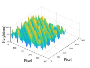
Topography: Topography of wafers and semiconductor devices is also an important application for white light interferometry. Through the white light interferometer, the three-dimensional topographic information of wafers and semiconductor devices can be obtained to further analyze their structural characteristics and performance.
Quality control: Quality control on the production line is also a key application of white light interferometer in semiconductor inspection. Through real-time monitoring and data analysis, white light interferometer can ensure stable quality and performance of semiconductor products, improve production efficiency and reduce production costs.
The application scenarios of POMEAS 3D white light interferometric profilers in semiconductor inspection are rich and varied, and their advantages in high-precision measurements, non-contact measurements and fast measurements make them an indispensable and important tool in the semiconductor manufacturing and inspection process.
Product recommendation
TECHNICAL SOLUTION
MORE+You may also be interested in the following information
FREE CONSULTING SERVICE
Let’s help you to find the right solution for your project!

 ASK POMEAS
  PRICE INQUIRY
  REQUEST DEMO/TEST
  FREE TRIAL UNIT
  ACCURATE SELECTION
 - APPICATION CASE
- RESOURCE CENTER
- DOWNLOAD CENTER
SOLUTIONS SUPPORT
- ZOOM LENS SELECTION TOOL
- TELECENTRIC LENS SELECTION TOOL
- FA LENS SELECTION TOOL
- ZOOM RATIO TABLE
- CERTIFIED MODEL
SELECTION TOOL
- WHY POMEAS
- FAQ
- PRIVACY POLICY
- TERMS OF USE
- DELIVERY & RETURN POLICY
CUSTOMER CARE
 ADDRESS
Add.:No.68, Chongwei Road, Baizhoubian, East district, Dongguan, China, 523000
CONTACT
 Tel:+ 86-0769-2266 0867
 Fax:+ 86-0769-2266 0867
 E-mail:marketing@pomeas.com

Wechat QR code
Software Copyright :2021SR0176001 抄袭必究, 技术支持:誉新源科技