


Chip Inspection and Guidance - Focus Laser Autofocus Microscopy System
Chip inspection is a complex and delicate process. Due to the tiny size of the product being inspected, multiple factors need to be considered when inspecting the chip to ensure the accuracy and reliability of the results. For example:
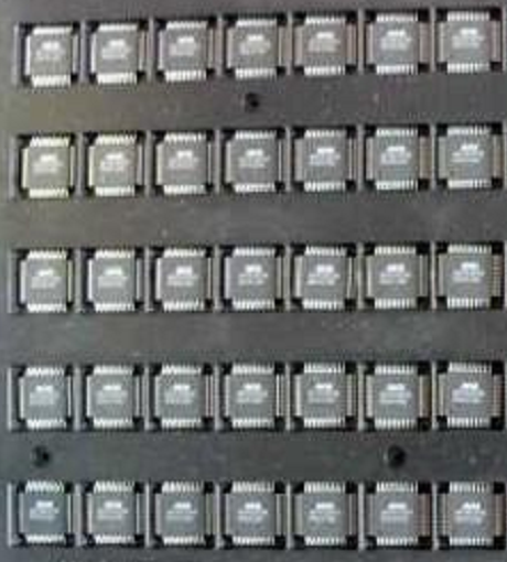
1, Complexity: the chip's internal structure is complex, containing a large number of transistors, resistors, capacitors and other components, as well as complex interconnections and logic circuits. This requires that the inspection process must be accurate and comprehensive, involving numerous electronic, circuit and device technology, requiring inspectors to have deep professional knowledge and skills.
2, Small Defects Detection: chip size is tiny, the defects on the corresponding very small, which puts forward high requirements for the resolution and sensitivity of the detection equipment. Even the smallest defects may affect the performance and stability of the chip, so it must be able to accurately detect and locate these defects.
3, The Impact Of Surface Characteristics: different materials and surface characteristics of the chip may require different detection methods and parameters. For example, some chip surfaces may have reflective, which will affect the accuracy of the detection results. Therefore, the detection process needs to take these factors into account and take appropriate measures to eliminate or reduce their impact.
4 Data Processing and Analysis: In the process of chip inspection, a large amount of data will be generated, how to quickly and accurately process and analyze these data is an important challenge. In addition, for some complex chips, pattern recognition, machine learning and other advanced data processing techniques may be required to assist detection.
5, light and Reflection Problems: in the use of optical technology for detection, light conditions and surface reflections and other issues may interfere with the detection results. Therefore, it is necessary to optimize the lighting conditions and use appropriate image processing algorithms to eliminate or reduce these interferences.
6, The Diversity Of Test Types: the chip test a variety of types, including sampling test and production of the full test and so on. Each type of test has its own specific objectives and requirements, and it is necessary to select appropriate testing methods and equipment according to different test types.
The POMEA Focus laser autofocus microscope is a high-precision, high-speed measurement device that offers significant advantages in the inspection of chips. Below:
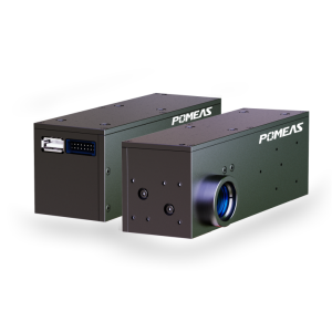
1. High-precision measurement: Focus laser autofocus microscope system adopts advanced laser technology and optical system, which is capable of realizing micron-level or even higher measurement precision. This makes it capable of accurately detecting tiny structures and defects on chips, providing reliable data support for chip manufacturing and quality control.
2. High-speed detection: The system's fast focusing speed enables it to quickly capture image information on the chip. This greatly reduces the inspection time and improves the production efficiency, especially suitable for large-scale chip production lines.
3. Co-axial focusing mode: Focus laser autofocus microscope system adopts co-axial focusing mode, which effectively solves the problem of occlusion when focusing. This enables the system to more accurately locate the target area on the chip, improving the accuracy and reliability of inspection.
4. Wide range of applications: As the Focus laser autofocus microscope system is characterized by high precision and high speed, it can be widely used in the inspection of various chips, including semiconductor chips, integrated circuit chips and so on. It can play an important role in both sample inspection at the R&D stage and quality monitoring on the production line.
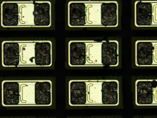
When inspecting chips, the Focus laser autofocus microscope system can realize non-contact inspection of microstructures and defects on the chip surface by precisely controlling the irradiation position and focal length of the laser beam. By collecting the reflected laser signals, the system can generate high-resolution images to further analyze and identify various features on the chip.

POMEAS Focus laser autofocus microscope has the advantages of high precision and high speed in chip inspection and has a wide range of application prospects. With the continuous development of science and technology, POMEAS Focus laser autofocus microscope will play a more and more important role in the field of chip manufacturing with its high precision and high speed microscopic inspection system.
Product recommendation
TECHNICAL SOLUTION
MORE+You may also be interested in the following information
FREE CONSULTING SERVICE
Let’s help you to find the right solution for your project!

 ASK POMEAS
  PRICE INQUIRY
  REQUEST DEMO/TEST
  FREE TRIAL UNIT
  ACCURATE SELECTION
 - APPICATION CASE
- RESOURCE CENTER
- DOWNLOAD CENTER
SOLUTIONS SUPPORT
- ZOOM LENS SELECTION TOOL
- TELECENTRIC LENS SELECTION TOOL
- FA LENS SELECTION TOOL
- ZOOM RATIO TABLE
- CERTIFIED MODEL
SELECTION TOOL
- WHY POMEAS
- FAQ
- PRIVACY POLICY
- TERMS OF USE
- DELIVERY & RETURN POLICY
CUSTOMER CARE
 ADDRESS
Add.:No.68, Chongwei Road, Baizhoubian, East district, Dongguan, China, 523000
CONTACT
 Tel:+ 86-0769-2266 0867
 Fax:+ 86-0769-2266 0867
 E-mail:marketing@pomeas.com

Wechat QR code
Software Copyright :2021SR0176001 抄袭必究, 技术支持:誉新源科技