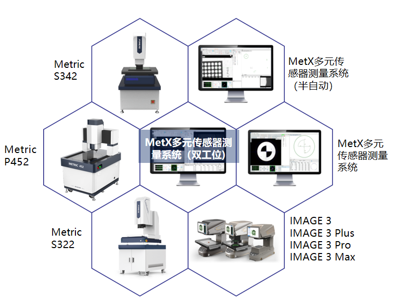
Multi-sensor measurement system has a wide range of application prospects in PCB inspection, which can help manufacturers to improve product quality and production efficiency, reduce production costs, and improve product reliability and stability.


Size Inspection: Multi-sensor measurement systems can acquire multiple parameters of a PCB, such as length, width, thickness, etc., from multiple sensors and measure them with high accuracy. This data can help manufacturers determine whether the PCB dimensions meet the design requirements and whether adjustments need to be made.
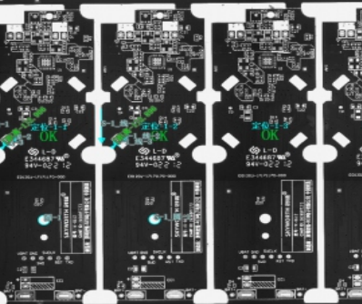
Surface defect detection: Multi-sensor measurement systems can acquire images of the PCB surface through image sensors and other devices, and use image processing techniques to detect the presence of defects on the surface, such as scratches, stains, and holes. These defects may cause the PCB to fail in subsequent use, so timely detection and treatment of these defects can improve product quality and reliability.
Solder joint inspection: Multi-sensor measurement systems can obtain information about solder joints on PCBs through infrared sensors, laser sensors, and other devices, and analyze them through algorithms to determine the quality of the solder joints. For example, the system can measure the shape, size, temperature and other parameters of the solder joints to determine whether the solder joints are well soldered and whether there are problems such as false soldering and cold soldering.
The application of multi-sensor measurement systems in PCB inspection requires selection and configuration based on specific inspection needs. Selecting the right optical measurement solution and data analysis technique is key to ensuring accuracy and reliability. At the same time, system integration and calibration are crucial steps to ensure the accuracy and repeatability of measurement results.
Detection program:
1, 130W pixel color digital camera;
2, PMS 6.5X continuous zoom lens;
3, five rings and eight zones white cold light source;
4, White high brightness parallel telecentric cold light source;
5, the lens comes with high brightness and high uniformity cold light source.

Multi-sensor measurement systems have other applications in PCB inspection, such as Optical Character Recognition (OCR) technology for recognizing markings and characters on PCBs to verify readability and traceability. Together, these technologies enable comprehensive and efficient PCB inspection that improves product quality and productivity.
Product recommendation
TECHNICAL SOLUTION
MORE+You may also be interested in the following information
FREE CONSULTING SERVICE
Let’s help you to find the right solution for your project!

- APPICATION CASE
- RESOURCE CENTER
- DOWNLOAD CENTER
SOLUTIONS SUPPORT
- ZOOM LENS SELECTION TOOL
- TELECENTRIC LENS SELECTION TOOL
- FA LENS SELECTION TOOL
- ZOOM RATIO TABLE
- CERTIFIED MODEL
SELECTION TOOL
- WHY POMEAS
- FAQ
- PRIVACY POLICY
- TERMS OF USE
- DELIVERY & RETURN POLICY
CUSTOMER CARE
 ADDRESS
Add.:No.68, Chongwei Road, Baizhoubian, East district, Dongguan, China, 523000
CONTACT
 Tel:+ 86-0769-2266 0867
 Fax:+ 86-0769-2266 0867
 E-mail:marketing@pomeas.com

Wechat QR code

 ASK POMEAS
  PRICE INQUIRY
  REQUEST DEMO/TEST
  FREE TRIAL UNIT
  ACCURATE SELECTION