


We often see autofocus technology used in a wide range of semiconductor manufacturing processes because semiconductor manufacturing requires technology for precise positioning and fast measurement.

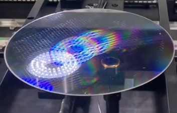
In the semiconductor chip manufacturing process, the measured position of the wafer needs to be aligned with the focus of the camera at all times. There are various ways of autofocusing, here we focus on the following two typical autofocus modes.
Passive Focus Seeking: This type of focusing should more accurately be described as focus seeking. Since the direction of focus is unknown, the wafer moves at a certain speed near the focal length of the camera while the camera continues to take successive images (similar to an MRI slice). The host computer commands the wafer to move to the appropriate position after finding the sharpest image. This focusing method has certain requirements on the minimum step and repeat positioning accuracy of the motion platform. However, due to the process characteristics of focus seeking, its yield is often not high.
Active Focus: Active focus is the real-time adjustment of the distance between the objective lens and the wafer to maintain optimal focus while the motion stage is moving in the XY direction. The distance information needs to be fed to the motion control system via mapping or feed-forward and commanded to the Z-direction actuator. This helps to increase machine throughput. However, it poses a challenge to the dynamic performance of the motion platform.
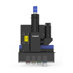
POMEAS Focus X laser autofocus microscope system is compact and adopts the co-axial focusing mode, which effectively solves the problem of occlusion when focusing; it has high focusing accuracy, fast focusing speed, stable and reliable product performance, and can be widely used in complex applications and environments.

Laser autofocus has a wide range of applications in semiconductor manufacturing and plays an important role in improving the precision, efficiency and stability of semiconductor manufacturing.
Product recommendation
TECHNICAL SOLUTION
MORE+You may also be interested in the following information
FREE CONSULTING SERVICE
Let’s help you to find the right solution for your project!

 ASK POMEAS
  PRICE INQUIRY
  REQUEST DEMO/TEST
  FREE TRIAL UNIT
  ACCURATE SELECTION
 - APPICATION CASE
- RESOURCE CENTER
- DOWNLOAD CENTER
SOLUTIONS SUPPORT
- ZOOM LENS SELECTION TOOL
- TELECENTRIC LENS SELECTION TOOL
- FA LENS SELECTION TOOL
- ZOOM RATIO TABLE
- CERTIFIED MODEL
SELECTION TOOL
- WHY POMEAS
- FAQ
- PRIVACY POLICY
- TERMS OF USE
- DELIVERY & RETURN POLICY
CUSTOMER CARE
 ADDRESS
Add.:No.68, Yongwei Road, Baizhoubian, Dongcheng District, Dongguan, China,523000
CONTACT
 Tel:+ 86-0769-2266 0867
 Fax:+ 86-0769-2266 0867
 E-mail:marketing@pomeas.com

Wechat QR code
Software Copyright :2021SR0176001 抄袭必究, 技术支持:誉新源科技