Difficulties in wafer surface inspection:
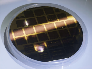

With the rapid development of semiconductor processes, the detection of wafer surface defects is facing more and more challenges. Wafer is the core component of semiconductor manufacturing, and its surface quality directly affects the performance and reliability of the chip.
1, the detection of high precision requirements: wafer surface defects are often very small size, and even reach the nanometer level, which requires detection equipment with very high resolution and accuracy.
2, fast detection: semiconductor manufacturing is a high-speed process, wafers need to be completed in a short period of time in a number of inspection links to ensure production efficiency and product quality.
3, defects of various types: the wafer surface defects may occur in many types, such as scratches, cracks, impurities, oxidation, etc., the detection of these defects requires different technical means and algorithms.
4, the complexity of the detection environment: wafer inspection process may be subject to a variety of external factors, such as temperature, humidity, light, etc., these factors will affect the accuracy of the test results.
Wafer surface inspection equipment:
In order to meet the high demands of wafer surface defect inspection, a variety of advanced inspection equipment has appeared on the market. The following are a few common types of wafer surface defect inspection equipment
1、Laser autofocus microscope system

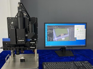
① Principle: Utilizing the self-focusing characteristics of the laser beam to achieve precise focus control, the image is captured by an industrial camera, and the laser sensor keenly senses the change in focal length, thus realizing auto-focus.
② Features: High precision, high efficiency, non-contact detection and other advantages, able to achieve micron-level detection accuracy. It is suitable for coating inspection, development and etching monitoring, impurity distribution inspection in wafer manufacturing process, and bump height and coplanarity inspection in chip packaging process.
2、4K zoom lens autofocus video microscope

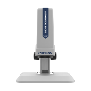
① Principle: Adopting 4K HD lens and zoom technology, it realizes high-definition observation of wafer surface by adjusting the magnification and focal length of the lens.
② Characteristics: Large target surface, high resolution, high precision, high efficiency, continuity and other advantages. It is able to capture the dust residue, oxidation, scratches, linear defects and other defects that exist in the process of wafer product fabrication faster and more clearly.
3、Spectral autofocus microscope system

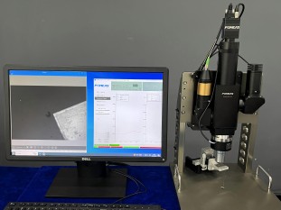
① Principle: Realize automatic focusing by analyzing spectral information, and utilize the absorption, reflection and transmission characteristics of light from different materials to achieve accurate inspection of wafer surfaces.
② Characteristics: It can provide rich spectral data to provide more comprehensive information for wafer inspection. It is suitable for accurate inspection of wafers made of different materials, and is especially good in complex inspection environments.
Product recommendation
TECHNICAL SOLUTION
MORE+You may also be interested in the following information
FREE CONSULTING SERVICE
Let’s help you to find the right solution for your project!

 ASK POMEAS
  PRICE INQUIRY
  REQUEST DEMO/TEST
  FREE TRIAL UNIT
  ACCURATE SELECTION
  ADDRESS
 Tel:+ 86-0769-2266 0867
 Fax:+ 86-0769-2266 0867
 E-mail:marketing@pomeas.com
