Semiconductor Wafer Inspection Background


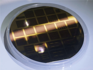
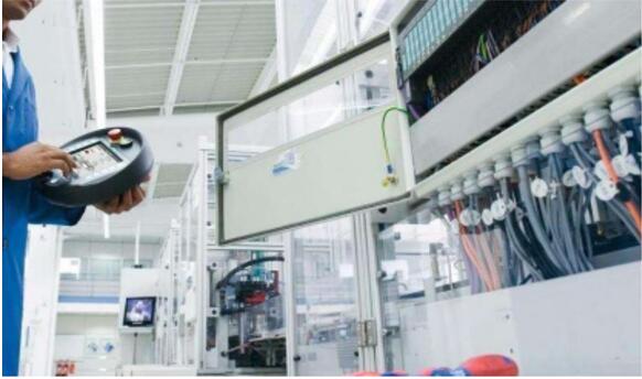
In the semiconductor manufacturing industry, wafer inspection is a key part of ensuring product quality and production efficiency. With the continuous development of semiconductor technology, the circuit pattern on the wafer is becoming more and more complex and the size is getting smaller and smaller, which puts forward higher requirements for the accuracy and efficiency of the inspection technology. Traditional inspection methods often rely on manual operation, which is not only time-consuming and labour-intensive, but also susceptible to the influence of human factors, resulting in the accuracy and consistency of the inspection results are difficult to ensure. Therefore, automated and intelligent wafer inspection systems have emerged, in which the automatic focusing system, as one of the core technologies, is of great significance for improving inspection accuracy and efficiency.
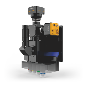
Autofocus system: Focus laser autofocus microscope system


The Focus laser autofocus microscopy system is an advanced autofocus technique that combines the principles of laser ranging and microscopic imaging to achieve high-precision, real-time focusing of tiny structures on the wafer surface. The system calculates the height information of the wafer surface by firing a laser beam to the wafer surface and receiving the reflected back laser signals, and calculates the height information of the wafer surface based on the time difference or phase difference of the signals. The system then automatically adjusts the focus of the microscope based on this information to ensure that the image is always clear and accurate.
Compared with traditional mechanical or manual focusing, the Focus laser autofocus microscope system has higher focusing accuracy and faster focusing speed. It can complete the focusing process in a very short time and is not affected by the height difference of the wafer surface, thus greatly improving the inspection efficiency and accuracy.
Advantages of Automatic Focusing System for Semiconductor Wafer Inspection
1、Ignore height difference: Focus laser autofocus microscope system can measure the height information of the wafer surface in real time, and automatically adjust the focus according to this information. Therefore, no matter how much height difference exists on the wafer surface, the system can ensure that the image is always clear and accurate. This feature makes the system in the detection of complex three-dimensional structure of the wafer has a significant advantage.
2、 Real-time focus: Due to the use of advanced laser ranging technology, Focus laser autofocus microscope system can be completed in a very short period of time focusing process. This means that during the inspection process, the system can track changes in the wafer surface in real time, and always maintain the best focus state. This feature is essential to improve inspection efficiency and accuracy.
3、Automatic follow focus: The system has an automatic follow focus function, which can automatically adjust the focus according to the height change of the wafer surface. This feature not only reduces the burden on the operator, but also improves the degree of automation and consistency of inspection. In a long time, high-volume inspection tasks, the automatic focusing system can always maintain stable detection performance.
Product recommendation
TECHNICAL SOLUTION
MORE+You may also be interested in the following information
FREE CONSULTING SERVICE
Let’s help you to find the right solution for your project!


 ASK POMEAS
  PRICE INQUIRY
  REQUEST DEMO/TEST
  FREE TRIAL UNIT
  ACCURATE SELECTION
  ADDRESS
 Tel:+ 86-0769-2266 0867
 Fax:+ 86-0769-2266 0867
 E-mail:marketing@pomeas.com
