


Spectral Confocal Sensors for Wafer Surface Topography Inspection Applications
Spectral Confocal Sensor Principle:


The principle of spectral confocal sensors is to use optical dispersion and confocal techniques to measure the position or shape of an object. As follows:
1, light source emission: the light emitted from the white LED light source is approximated as a point light source after passing through the optical fibre coupler.
2, light processing: after collimation and dispersive objective lens focusing, the light occurs spectral dispersion, the formation of a continuous monochromatic light focus on the optical axis, and each monochromatic light focus to the object to be measured at different distances.
3, reflection and reception: when the measured object is in a position within the measurement range, only a certain wavelength of light focused on the measured surface, the wavelength of light due to meet the confocal conditions, can be reflected from the surface of the object to be measured back to the optical fibre coupler and into the spectrometer. While other wavelengths of light on the surface of the object under test is in the defocused state, the distribution of reflected light back at the light source is much larger than the diameter of the fibre core, so most of the light can not enter the spectrometer.
4, data processing: the spectrometer decodes the received light to get the wavelength value at the maximum light intensity, and then according to the pre-calibrated wavelength and distance correspondence, you can measure the distance value corresponding to the target.
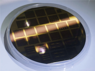
Applications in wafer surface topography inspection

Surface defect detection:
(1) Scratch detection: Scratches may occur on wafers during production, transport or processing. Spectral confocal sensors can scan the wafer surface with high precision and detect tiny scratches. These scratches may affect the performance and reliability of the wafer, and can be detected and acted upon in time through detection.
(2) Pit and bump detection: Defects such as pits or bumps may appear on the wafer surface, and these defects can affect the manufacturing quality of the chip. Spectral confocal sensors can detect pits and bumps on the wafer surface, providing accurate three-dimensional topographical information to help engineers assess the extent and impact of defects.
(3) Particle contamination detection: During the wafer fabrication process, there may be particle contaminants attached to the wafer surface. Spectral confocal sensors can detect the location, size and shape of these particle contaminants, providing a basis for wafer cleaning and quality control.
Flatness test:
The flatness of a wafer is one of the most important indicators of its quality. Spectral confocal sensors can quickly and accurately measure the flatness of the wafer surface and detect the degree of undulation and bending of the wafer surface. Through the detection of flatness, wafers that meet the requirements can be screened to improve the yield of chip manufacturing.
Step height measurement:
During semiconductor manufacturing, different structures and layers are formed on wafers, and the height of the steps between these structures and layers needs to be precisely controlled. Spectral confocal sensors can measure the height of steps on wafers, providing data to support process control and quality inspection.
Roughness measurement:
The roughness of the wafer surface affects the performance and reliability of the chip. Spectral confocal sensors can measure the roughness of the wafer surface and provide detailed surface topography information. By detecting the roughness, the processing quality of the wafer can be assessed and the processing process can be optimised.
Three-dimensional morphological reconstruction:
Spectral confocal sensors can scan the wafer surface in the full field and acquire a large amount of 3D topography data. By processing and analysing this data, the 3D topography of the wafer surface can be reconstructed, providing engineers with intuitive visual information to help them better understand the surface characteristics and quality conditions of the wafer.
Product recommendation
TECHNICAL SOLUTION
MORE+You may also be interested in the following information
FREE CONSULTING SERVICE
Let’s help you to find the right solution for your project!

 ASK POMEAS
  PRICE INQUIRY
  REQUEST DEMO/TEST
  FREE TRIAL UNIT
  ACCURATE SELECTION
 - APPICATION CASE
- RESOURCE CENTER
- DOWNLOAD CENTER
SOLUTIONS SUPPORT
- ZOOM LENS SELECTION TOOL
- TELECENTRIC LENS SELECTION TOOL
- FA LENS SELECTION TOOL
- ZOOM RATIO TABLE
- CERTIFIED MODEL
SELECTION TOOL
- WHY POMEAS
- FAQ
- PRIVACY POLICY
- TERMS OF USE
- DELIVERY & RETURN POLICY
CUSTOMER CARE
 ADDRESS
Add.:No.68, Chongwei Road, Baizhoubian, East district, Dongguan, China, 523000
CONTACT
 Tel:+ 86-0769-2266 0867
 Fax:+ 86-0769-2266 0867
 E-mail:marketing@pomeas.com

Wechat QR code
Software Copyright :2021SR0176001 抄袭必究, 技术支持:誉新源科技